Super-junction device and method for manufacturing same

A super junction and device technology, applied in semiconductor/solid-state device manufacturing, semiconductor devices, electrical components, etc., can solve the problems of device recovery current change, diode hard reverse recovery characteristics, device failure, etc.

Active Publication Date: 2015-03-18
SHANGHAI HUAHONG GRACE SEMICON MFG CORP
View PDF6 Cites 0 Cited by
  • Summary
  • Abstract
  • Description
  • Claims
  • Application Information

AI Technical Summary

Problems solved by technology

[0004] In the super junction process, due to the use of alternating P / N thin layers, the body diode of the super junction device, that is, the diode formed between the P-type semiconductor thin layer and the N-type semiconductor thin layer, can operate at a lower voltage such as 50 volts Vds The P-type semiconductor thin layer and the N-type semiconductor thin layer will be completely depleted, which makes the diode have a very hard reverse recovery characteristic. This hard reverse recovery characteristic causes the recovery current of the device to change sharply, resulting in Very high voltage overshoot can cause device failure
At the same time, due to the sharp change of current and voltage, that is, high di / dt and dv / dt will cause electromagnetic interference (EMI-ELEACTROMAGENETIC INTERFERENCE) in the circuit, which will affect the system and even exceed the EMI standard. In this regard, super junction The device is not as good as the conventional MOSFET device, because the depletion of the N-drift region of the conventional MOSFET device always expands with the increase of the voltage (Vds), and the reverse recovery characteristic is soft

Method used


Image

  • Super-junction device and method for manufacturing same
  • Super-junction device and method for manufacturing same
  • Super-junction device and method for manufacturing same

Examples


Embodiment Construction

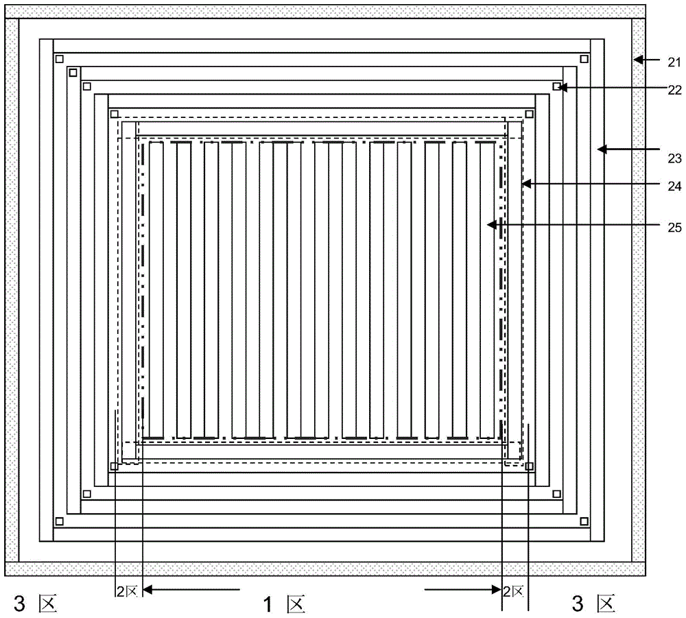
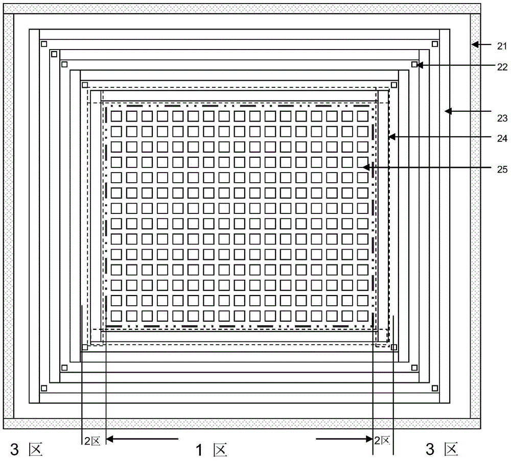
[0054] Such as figure 1 Shown is the top view of the existing super junction device Figure 1 . In the top view, the embodiment of the present invention can be divided into zone 1, zone 2 and zone 3. Region 1 is the middle region of the super junction device, which is the current flow region, and the current flow region includes alternately arranged P-type regions 25 and N-type regions, and the P-type regions 25 are also P-type regions formed in the current flow region. The N-type thin layer, the N-type region is also the N-type thin layer formed in the current flow region; in the current flow region, the current will pass through the N-type region from the source to the drain through the channel, and the The P-type region 25 is in the reverse cut-off state and forms a depletion region together with the N-type region to withstand voltage. Regions 2 and 3 are the terminal protection structure regions of the super junction device. The terminal protection structure does not pr...


PUM

PropertyMeasurementUnit
electrical resistivityaaaaaaaaaa
thicknessaaaaaaaaaa

Abstract

The invention discloses a super-junction device. A current flow region comprises a plurality of N-type thin layers and P-type thin layers which are arranged alternatively. The N-type thin layers comprise two types, and both the two types of N-type thin layers comprise a high-resistance part in the middle and low-resistance parts at the two sides. The charge of the first type of N-type thin layers and that of the P-type thin layers are in balance. The second type of N-type thin layers has a wider high-resistance part, and the charge of the second type of N-type thin layers and that of the P-type thin layers are not in balance. After the P-type thin layers horizontally deplete the second type of N-type thin layers, a P well on the top of the N-type thin layers vertically depletes the high-resistance parts of the second type of N-type thin layers in a gradually expanding way with the increase of reverse bias voltage. The invention further discloses a method for manufacturing the super-junction device. The reverse recovery characteristic of the device can be improved, and the conduction resistance is low.

Description

technical field [0001] The invention relates to the field of semiconductor integrated circuit manufacturing, in particular to a super junction device; the invention also relates to a manufacturing method of the super junction device. Background technique [0002] The super junction MOSFET adopts a new voltage-resistant layer structure, and uses a series of alternately arranged P-type semiconductor thin layers and N-type semiconductor thin layers to combine the P-type semiconductor thin layers and N-type semiconductor thin layers at a lower voltage in the off state. The thin layer of semiconductor is depleted to achieve mutual compensation of charges, so that the thin layer of P-type semiconductor and thin layer of N-type semiconductor can achieve high breakdown voltage under high doping concentration, so as to obtain low on-resistance and high breakdown at the same time voltage, breaking the theoretical limit of traditional power MOSFETs. In U.S. Patent US5216275, the above...

Claims


Application Information

Patent Timeline
Patent Type & Authority Applications(China)
IPC IPC(8): H01L29/78H01L29/06H01L21/336
CPCH01L29/0634H01L29/66477H01L29/78
Inventor 肖胜安
Owner SHANGHAI HUAHONG GRACE SEMICON MFG CORP
Why Eureka
Try Eureka