CSP type mems package and production method based on custom lead frame

A lead frame and production method technology, applied in the field of CSP type MEMS packages, can solve the problems of cut-off and distortion of output signals, and achieve the effects of ensuring detection accuracy and eliminating dryness

Active Publication Date: 2017-04-05
TIANSHUI HUATIAN TECH
View PDF5 Cites 0 Cited by
  • Summary
  • Abstract
  • Description
  • Claims
  • Application Information

AI Technical Summary

Problems solved by technology

Although the MEMS chip has a strong signal detection function, it will be affected by the additional inductance, capacitance, resistance of the package itself and the interference signal of the environment in actual use, causing the output signal to be cut off or distorted.

Method used


Image

  • CSP type mems package and production method based on custom lead frame
  • CSP type mems package and production method based on custom lead frame
  • CSP type mems package and production method based on custom lead frame

Examples


Embodiment 1

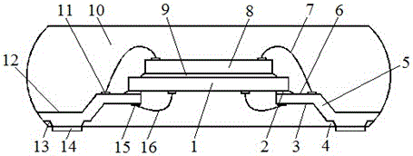
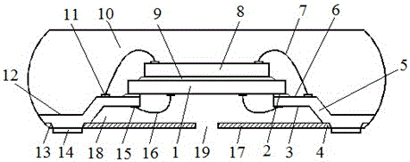
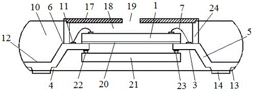
[0045]According to customer needs, design multi-row matrix CSP lead frame drawings with different structures and specifications, and make 8-row matrix CSP custom lead frames with no carrier-wing gull-shaped inner pins. The front and back of the inner pins are in addition to electroplated copper. , but also silver-plated; use an 8-inch to 12-inch thinning machine to thin the wafer, the wafer with bumps is thinned to 150 μm, and the wafer without bumps is thinned to 130 μm; during the thinning process The rough grinding speed is 6μm / s, the fine grinding speed is 0.15μm / s, and the polishing speed is 0.05μm / s; at the same time, the anti-warping process is adopted: use A-WD-300TXB dicing machine to scribe the thinned wafer, and scribe During the dicing process, the anti-fragmentation double-knife process is used for scribing, and the dicing feed speed is ≤10mm / s, and the required MEMS IC chip and VGA amplifier chip are formed by cutting and separating; on the chip bonding machine, t...

Embodiment 2

[0047] According to the chip and customer needs, design multi-row matrix CSP lead frame drawings with different structures and specifications, and make 16 rows of matrix CSP custom lead frames without carrier-wing gull-shaped inner pins, and remove the electroplating on the front and back of the inner pins In addition to copper, nickel-palladium-gold pads should also be plated; the wafers are thinned using an 8-inch to 12-inch thinning machine, and the wafers with bumps are thinned to 200 μm, and the wafers without bumps are thinned to 155μm; during the thinning process, the rough grinding speed is 6μm / s, the fine grinding speed is 0.15μm / s, and the polishing speed is 0.05μm / s; at the same time, the anti-warping process is adopted: then, the A-WD-300TXB dicing machine is used The wafer is diced, and the anti-fragmentation double-knife process is used for slicing during the slicing process. The slicing feed speed is ≤10mm / s, and the MEMS IC chip and VGA amplifier chip are formed...

Embodiment 3

[0049] According to the chip and customer needs, design multi-row matrix CSP lead frame drawings with different structures and specifications, and make 12 rows of matrix CSP custom lead frames with no carrier-wing gull-shaped inner pins, and remove the electroplating on the front and back of the inner pins In addition to copper, the UBM metal layer required for flip-chip packaging is also electroplated; the wafer is thinned using an 8-inch to 12-inch thinning machine, and the wafer with bumps is thinned to 175 μm, and the wafer without bumps Thinning to 180 μm; during the thinning process, the rough grinding speed is 6 μm / s, the fine grinding speed is 0.15 μm / s, and the polishing speed is 0.05 μm / s; at the same time, the anti-warping process is adopted: then, A-WD-300TXB dicing machine is used The thinned wafer is diced. During the dicing process, the anti-fragmentation double-knife process is used for slicing. The scribing speed is ≤10mm / s, and the required MEMS IC chip and VG...


PUM


Abstract

A CSP-type MEMS package based on a customized lead frame and its production method. The upper surface of the inner pin of the package is flip-mounted with a MEMS chip with bumps, and the MEMS chip is connected to the pad on the back of the inner pin; the MEMS chip is pasted with The first VGA amplifier chip, the first VGA amplifier chip is connected to the upper surface of the inner pin; the metal layer of the bottom pin is provided on the bottom surface of the bottom pin; the lead frame is plastic-sealed with a first plastic package, and all devices are plastic-sealed on the first Inside the plastic package, only the metal layer of the pins on the bottom surface is exposed outside the first plastic package. Preparation of lead frame, wafer thinning dicing, pasting chip, wire bonding, plastic packaging and other processes to make CSP type MEMS package based on customized lead frame. The package can eliminate interference, ensure the accuracy of MEMS chip signal detection, reduce the impact of the additional package itself and parasitic inductance, capacitance, resistance and environmental interference on the signal, and prevent output signal cut-off, distortion or gain.

Description

technical field [0001] The invention belongs to the technical field of semiconductor manufacturing, and relates to a CSP type MEMS package based on a customized lead frame, and also relates to a production method of the package. Background technique [0002] CSP (Chip Scale Package, the same below), that is, chip-scale package, this package is a thin, micro package developed on the basis of TSOP and BGA. CSP can achieve a package with a ratio of chip area to package area exceeding 1:1.14, and its package area is about 1 / 3 of that of ordinary BGA, which is only equivalent to 1 / 6 of the package area of ​​TSOP memory chips. CSP is not only small in size, but also thinner. The most effective heat dissipation path from the substrate to the heating element is often only 0.2mm, which greatly improves the reliability of the long-term operation of the memory chip, the line impedance is significantly reduced, and the chip speed is also increased. increase in magnitude. [0003] In t...

Claims


Application Information

Patent Timeline
Patent Type & Authority Patents(China)
IPC IPC(8): H01L23/495H01L21/60
CPCH01L2924/181B81B7/00H01L23/31H01L23/495H01L2224/16245H01L2224/32145H01L2224/32245H01L2224/48091H01L2224/48247H01L2224/73265H01L2924/00014H01L2924/00H01L2924/00012
Inventor 慕蔚邵荣昌李习周张易勒胡魁
Owner TIANSHUI HUATIAN TECH
Why Eureka
Try Eureka