Wireless energy transmission lighting system and preparation method of chip-level lighting device thereof

A wireless energy transmission and wireless energy technology, applied in the field of LED light sources, can solve the problems of GaN material-based system integration and other problems, and achieve the effect of non-contact electrical injection and large development space

Active Publication Date: 2016-10-19
INST OF SEMICONDUCTORS - CHINESE ACAD OF SCI
View PDF6 Cites 2 Cited by
  • Summary
  • Abstract
  • Description
  • Claims
  • Application Information

AI Technical Summary

Problems solved by technology

Some scientific research institutions in the world have tried one-to-one integration of GaAs, GaP and other light-emitting chips and power chips, but have not carried out GaN material-based system integration. GaN material-based system integration technology can form functional systems

Method used


Image

  • Wireless energy transmission lighting system and preparation method of chip-level lighting device thereof
  • Wireless energy transmission lighting system and preparation method of chip-level lighting device thereof

Examples


Embodiment Construction

[0024] In order to make the object, technical solution and advantages of the present invention clearer, the present invention will be described in further detail below in conjunction with specific embodiments and with reference to the accompanying drawings.

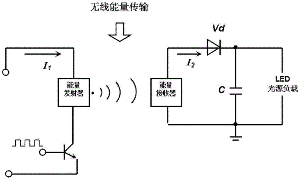
[0025] figure 1 is the equivalent circuit diagram of the wireless energy transmission lighting system of the present invention, such as figure 1 As shown, the wireless energy transmission lighting system includes a wireless energy sending device (such as figure 1 shown in the left half of the circuit) and wireless energy receiving and lighting devices (such as figure 1 shown in the right half of the circuit), where:

[0026] The wireless energy transmitting device is used to convert electric energy into free energy that can be freely propagated in space, and transmit the free energy by means of wireless energy transmission;

[0027] Wherein, the wireless energy transmission method includes one of electromagnetic induct...


PUM


Abstract

The invention discloses a wireless energy transmission light-emitting system. The system comprises a wireless energy emitting device and a wireless energy receiving and light-emitting device, wherein the wireless energy emitting device is used for converting electric energy into free energy capable of being freely transmitted in a spatial range and emitting the free energy out in a wireless energy transmission mode; the wireless energy receiving and light-emitting device is used for receiving the free energy freely transmitted in the spatial range and converting the received free energy into electric energy capable of being used by a light-emitting device and then the light-emitting device is driven to emit light. The wireless energy transmission technology is used, a metal electrode process in the traditional chip process technology is omitted, and well non-contact electric injection can still be conducted after the design size of a chip is greatly reduced. The wireless electric drive chip technology will have large development space whether in the chip research technological field or the chip application technological field.

Description

technical field [0001] The invention relates to the field of LED light source technology and the field of semiconductor device manufacturing technology, in particular to a wireless energy transmission lighting system and a method for preparing a chip-level lighting device thereof. Background technique [0002] Miniaturized LED light-emitting chips in the visible light band have broad application space in many fields, such as micro-display, high-definition display, neuron stimulation, fluorescence detection and other application fields. However, in these fields, LEDs are required to have a certain light output power, uniform light emission, stable light emission, high reliability, and convenient manufacture. The PN positive and negative electrodes of the LED chip with the traditional front-mount structure and the flip-chip structure are on the same side, and the PN electrodes of the LED light-emitting chip with the vertical structure are on both sides of the chip. But at pre...

Claims


Application Information

Patent Timeline
Patent Type & Authority Patents(China)
IPC IPC(8): H01L31/14H01L31/153H01L31/18H01L33/06
CPCH01L31/14H01L31/153H01L31/18H01L31/1864H01L33/06Y02P70/50
Inventor 詹腾马骏王钦金伊晓燕王国宏李晋闽
Owner INST OF SEMICONDUCTORS - CHINESE ACAD OF SCI
Why Eureka
Try Eureka