Low-thermoelectrical-potential scanning switch terminal connection mechanism based on flexible printed circuit board

A flexible circuit board, scanning switch technology, applied in the direction of electrical switches, circuits, connections, etc., can solve the problems of many thermoelectric potentials, easy signal interference, complex contact circuits, etc., to simplify the circuit, save direct welding, and avoid the circuit. the effect of interference

Active Publication Date: 2015-03-25
CHINA JILIANG UNIV
3 Cites 1 Cited by

AI-Extracted Technical Summary

Problems solved by technology

[0004] In order to solve the above-mentioned problems such as complex contact circuit, easy signal interference, and many thermoelectric potentials, the present invention provides a low thermal potential scanning switch terminal connection mechanism based on a flexible circuit board, which uses an FPC flexible circuit boa...

Abstract

The invention discloses a low-thermoelectrical-potential scanning switch terminal connection mechanism based on a flexible printed circuit board. The two side faces of the FPC board are bent and provided with a PCB and a rear panel respectively, and relays are installed on the PCB. Two signal pins of each relay penetrate through corresponding through grooves of the PCB and are welded to the FPC board, other pins, except the two signal pins, of each relay are directly welded to the PCB, the rear panel is provided with binding posts corresponding to the relays, and internal umbrella-shaped wiring ends of the binding posts penetrate through the rear panel and are connected with the FPC. By means of the FPC board, electric connection of the low-thermoelectrical-potential binding posts of the rear panel and the relays on the PCB is achieved. Circuits are simplified, interference between signals is reduced, and part of thermoelectrical potential generated due to welding between the PCB and the relays is avoided.

Application Domain

Coupling device connectionsPrinted circuits +1

Technology Topic

Printed circuit boardEngineering +5

Image

  • Low-thermoelectrical-potential scanning switch terminal connection mechanism based on flexible printed circuit board
  • Low-thermoelectrical-potential scanning switch terminal connection mechanism based on flexible printed circuit board
  • Low-thermoelectrical-potential scanning switch terminal connection mechanism based on flexible printed circuit board

Examples

  • Experimental program(1)

Example Embodiment

[0021] The present invention will be described in further detail below in conjunction with the accompanying drawings and specific embodiments.
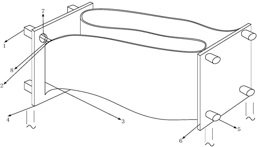
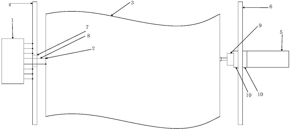
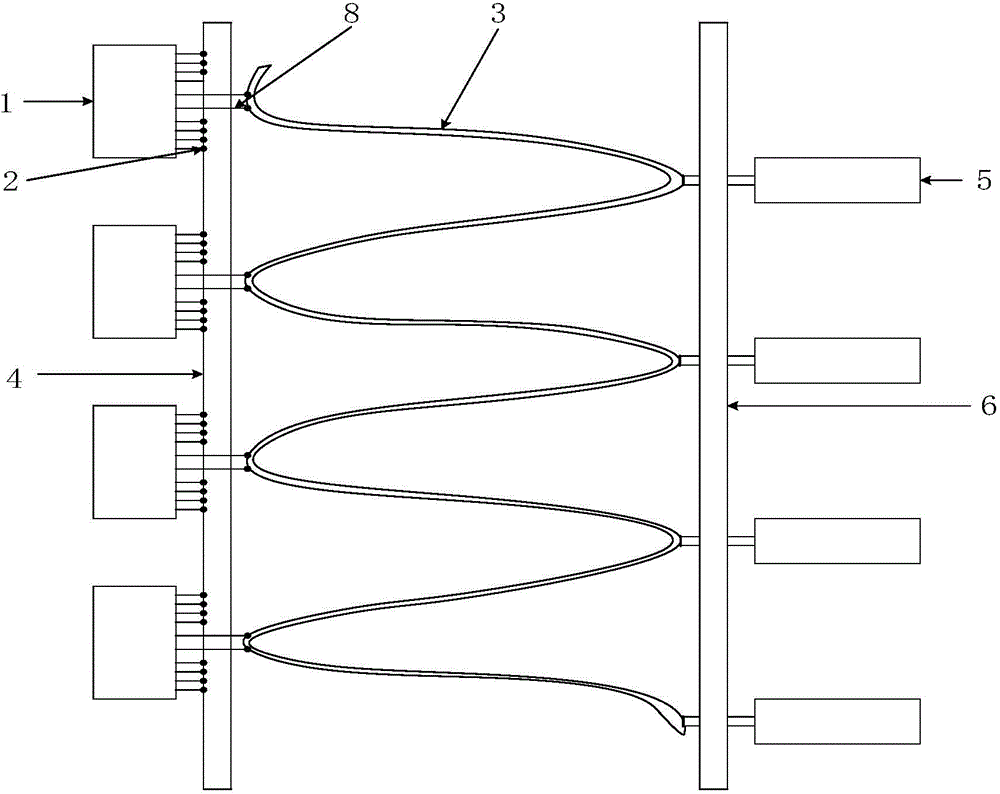
[0022] like figure 1 and figure 2 As shown, the present invention mainly includes the relay to be controlled in the scan switch, the PCB circuit board 4 , the FPC flexible circuit board 3 , the rear panel 6 and the low thermal potential terminal post 5 . like image 3 As shown, a PCB circuit board 4 and a rear panel 6 are respectively installed on both sides of the wave-shaped FPC flexible circuit board 3, and an FPC flexible circuit board 3 is installed between the PCB circuit board 4 and the rear panel 6, and the PCB circuit board 4 is installed with a relay 1, and the two signal pins 8 of the relay 1 are connected to the FPC flexible circuit board 3 through the through slot 7 of the corresponding PCB control circuit board 4, so that the signal pins can pass through it. Solder joint 2 is produced by direct welding between the relay and one end of the FPC flexible circuit board; other pins of the relay 1 except the two signal pins 8 are directly welded with the PCB control circuit board 4, and the wiring corresponding to the relay 1 is installed on the rear panel 6 Column 5, such as figure 2 As shown, the internal umbrella-shaped terminal of the terminal 5 is located on the left and connected to the FPC flexible circuit board 3 through the rear panel 6, and the external lead connection terminal of the terminal 5 is located on the right.
[0023] like figure 2 As shown, the middle part of the terminal 5 is fastened on the rear panel 6 by a nut 9, the middle part of the terminal 5 is provided with threads, and the nut 9 is connected to the middle part of the terminal 5, between the terminal 5 and the rear panel 6, between the nut 9 and the rear panel 6 are all sleeved with insulating spacers 10.
[0024] The two signal pins 8 of the relay 1 are soldered to the FPC flexible circuit board 3 respectively, such as figure 2 As shown in the welding spot 2 , the inner umbrella-shaped terminal of the terminal 5 is welded to the FPC flexible circuit board 3 .
[0025] like figure 1 As shown, the array of relays 1 is installed on the PCB circuit board 4 at even intervals, and the array of binding posts 5 is installed on the rear panel 6 at intervals. The array of relays 1 is the same as the array of each binding post 5 .
[0026] The aforementioned rear panel 6 is a metal panel, which is the rear panel of the chassis, and the pads on the FPC flexible circuit board 3 are plated with gold.
[0027] The insulating gasket 10 can adopt plastic insulating material.
[0028] The array of relay 1 is at least a 2×2 array. Relay 1 can be a magnetic latching relay. The magnetic latching relay is not welded with the control PCB circuit board, and each relay will reduce two signal pins and two PCB circuit boards. Solder joints, the N relays of the array reduce 2N solder joints.
[0029] The preferred number of detected relays is 1-128, and the preferred number of detected rear panel binding posts is 72.
[0030] Embodiments of the present invention and specific implementation work process are as follows:
[0031] like Figure 4 As shown, the present invention connects the relays on the PCB circuit board and the terminal posts on the rear panel through the FPC flexible circuit board: the relays form a matrix form of a 4×4 array, and an ellipse is opened on the PCB circuit board corresponding to the side of the relay. Through slots, so that the two signal pins of the relay can just pass through completely. There are 16 through slots for 16 relays, so as to ensure that each relay signal pin can just pass through. The wavy FPC flexible circuit board is welded, and each relay has two solder joints with the FPC flexible circuit board. The remaining pins on the relay are directly soldered to the PCB circuit board.
[0032] Corresponding to the 16 relays on the PCB circuit board, there are also 16 terminal posts installed on the rear panel. The plastic insulating gaskets are used to insulate the terminal posts from the metal rear panel. The binding posts are fixed on the metal rear panel, and one end of the umbrella mechanism is directly welded to the FPC flexible circuit board to generate solder joints. In this way, the FPC flexible circuit board connects the PCB circuit board relay and the terminal post on the rear panel together, so that the signal is successfully transmitted and the electrical characteristics are realized.
[0033] Therefore, the advantage of the FPC flexible circuit board of the present invention is that signals can circulate on the FPC flexible circuit board. Compared with the existing PCB circuit board and the metal back panel connected by cables or pins, the flexible circuit board can be folded into waves shape, easy to install; moreover, the opening of the slot on the PCB of the present invention allows the relay signal pins to just pass through, compared with the existing relay signal pins that are directly welded to the PCB circuit board, this will reduce the introduction of two solder joints and increase The thermoelectric potential and contact potential are understood, which has significant technical effects.
[0034] The above specific embodiments are used to explain the present invention, rather than to limit the present invention. Within the spirit of the present invention and the protection scope of the claims, any modification and change made to the present invention will fall into the protection scope of the present invention.

PUM

no PUM

Description & Claims & Application Information

We can also present the details of the Description, Claims and Application information to help users get a comprehensive understanding of the technical details of the patent, such as background art, summary of invention, brief description of drawings, description of embodiments, and other original content. On the other hand, users can also determine the specific scope of protection of the technology through the list of claims; as well as understand the changes in the life cycle of the technology with the presentation of the patent timeline. Login to view more.

Similar technology patents

Charging control method and device

Owner:XIAN ZHONGXING NEW SOFTWARE

Fan speed-adjusting circuit

Owner:GUANGZHOU PENGLIN LIGHTING CO LTD

High-reliability and high-luminous-efficiency LED (light-emitting diode) street lamp

InactiveCN103982845Areduce feverDispersed heat source
Owner:FOSHAN BAOYINGLI HARDWARE

Electric power engineering distribution box

InactiveCN111755968AEasy wiringAvoid Wiring Mistakes
Owner:安徽盛琛电力工程有限公司

Classification and recommendation of technical efficacy words

  • Avoid wiring mistakes

Electric power engineering distribution box

InactiveCN111755968AEasy wiringAvoid Wiring Mistakes
Owner:安徽盛琛电力工程有限公司
Why Eureka
Try Eureka