Circuit board impedance line compensation method and device

A compensation method and compensation device technology, which is applied in the field of circuit board impedance line compensation and circuit board impedance line compensation device, can solve problems such as the mismatch between the impedance line width and the thinnest line width, and affect the characteristic impedance value, so as to avoid transmission Signal distortion, improve work efficiency, improve the effect of mismatching impedance line width and the thinnest line width

Active Publication Date: 2015-03-25
ZHUHAI FOUNDER TECH HI DENSITY ELECTRONICS +1
View PDF2 Cites 25 Cited by
  • Summary
  • Abstract
  • Description
  • Claims
  • Application Information

AI Technical Summary

Problems solved by technology

[0008] The traditional impedance line compensation method is to perform indiscriminate compensation on the overall line width containing impedance line according to factors such as the completed surface copper, the minimum line width / line spacing in the board, etc. Wide, part of the line width is not enough, resulting in the mismatch between the line width of the impedance line and the thinnest line width, and affecting the characteristic impedance value

Method used


Image

  • Circuit board impedance line compensation method and device
  • Circuit board impedance line compensation method and device
  • Circuit board impedance line compensation method and device

Examples


Embodiment Construction

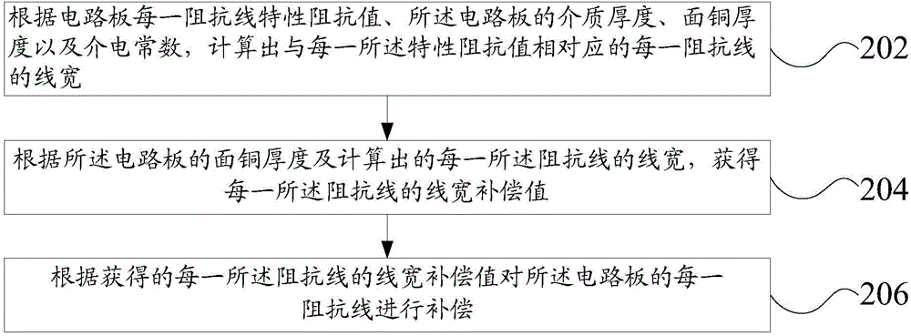
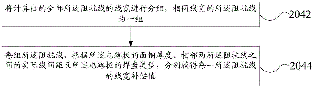
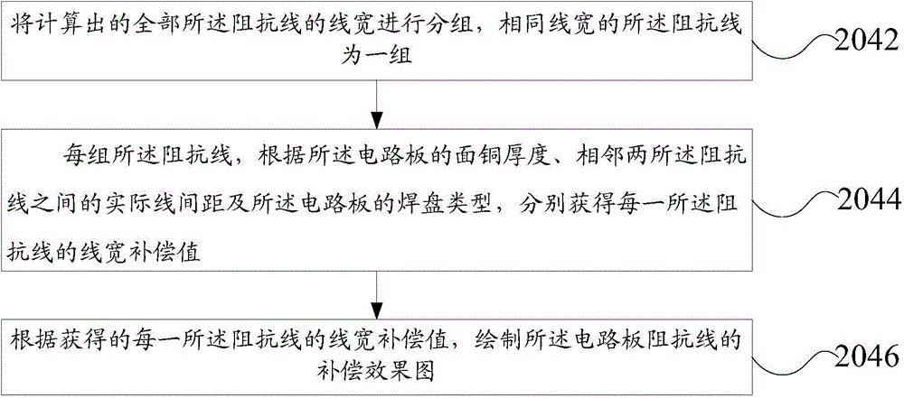
[0052] In order to understand the above-mentioned purpose, features and advantages of the present invention more clearly, the present invention will be further described in detail below in conjunction with the accompanying drawings and specific embodiments. It should be noted that, in the case of no conflict, the embodiments of the present application and the features in the embodiments can be combined with each other.

[0053] In the following description, many specific details are set forth in order to fully understand the present invention. However, the present invention can also be implemented in other ways than described here. Therefore, the protection scope of the present invention is not limited by the specific implementation disclosed below. Example limitations.

[0054] A frame-type coating film preparation device for preparing a coating film sample of a high-build sand-wall-like coating according to some embodiments of the present invention will be described below wi...


PUM


Abstract

The invention provides a circuit board impedance line compensation method and device. The circuit board impedance line compensation method includes the following steps that 202, the line width of each impedance line corresponding to each characteristic impedance value is calculated according to the characteristic impedance value of each impedance line of a circuit board, the dielectric thickness of the circuit board, the thickness of face copper and a dielectric constant; 204, the line width compensation value of each impedance line is obtained according to the thickness of the face copper of the circuit board and the calculated line width of each impedance line; 206, compensation is conducted on the impedance lines of the circuit board according to the obtained line width compensation value of each impedance line. According to the circuit board impedance line compensation method, the corresponding line width compensation values of all the impedance lines can be obtained at the same time, the circuit board compensation device can be used for fast conducting compensation on the line widths of all the impedance lines of the circuit board, and the production efficiency is improved effectively.

Description

technical field [0001] The invention relates to the field of circuit board production and manufacturing, and more specifically, relates to a circuit board impedance line compensation method and a circuit board impedance line compensation device. Background technique [0002] With the development of PCB (circuit board) towards the direction of fine wiring, miniaturization and high integration, new requirements are put forward for the impedance control of circuit board: [0003] 1. Refinement of impedance lines is required; [0004] 2. The dielectric thickness of the impedance line is required to be thin; [0005] 3. The tolerance requirements for impedance lines are stricter; [0006] 4. It is required that the surface roughening of the impedance lines is small and the etching factor is good. [0007] Impedance control includes characteristic impedance control and differential impedance control. Among them, characteristic impedance refers to the common effect of resistanc...

Claims


Application Information

Patent Timeline
Patent Type & Authority Applications(China)
IPC IPC(8): H05K3/00H05K1/02
CPCH05K1/0253H05K3/0005
Inventor 卓丽卿
Owner ZHUHAI FOUNDER TECH HI DENSITY ELECTRONICS
Why Eureka
Try Eureka