Efficient clock input control circuit
A clock input and control circuit technology, applied in the field of integrated circuits and memory, can solve the problems of inability to generate an internal clock signal ACT, and the memory cannot work, and achieve the effect of high efficiency and high circuit reliability.
- Summary
- Abstract
- Description
- Claims
- Application Information
AI Technical Summary
Problems solved by technology
Method used
Image

Examples
Embodiment Construction
[0024] The present invention will be described in detail below with reference to the accompanying drawings and in combination with embodiments.
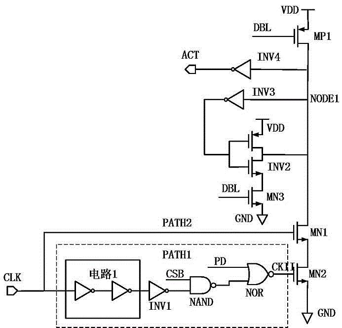
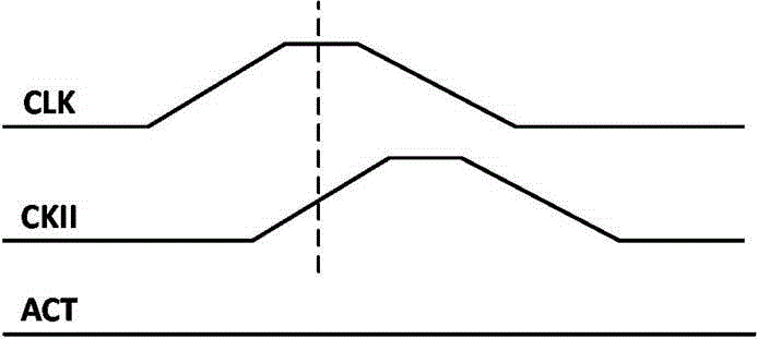
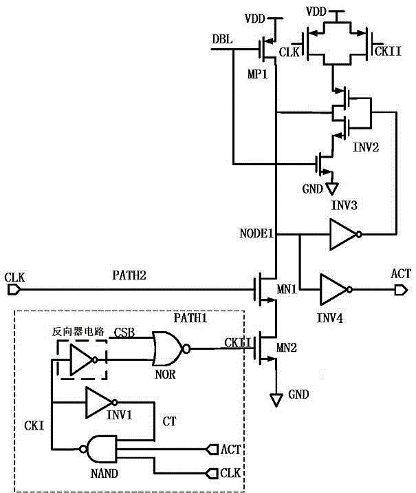
[0025] Such as image 3 As shown, an efficient and reliable clock input control circuit in the embodiment of the present invention includes a feedback loop of the internal clock ACT signal of the memory, and generates CKII and CLK signals through the PATH1 channel to control the NMOS transistors MN1 and MN2 together. When MN1 and When MN2 is turned on, NODE1 is pulled low and ACT goes high. When the DBL signal is low, the PMOS transistor MP1 is turned on, NODE1 is pulled high, and the ACT signal is pulled low through the inverter INV4. In addition, the potential of the NODE1 node is always clamped at high or low through the inverters INV2 and INV3. Unlike the previously mentioned circuits, image 3 The PATH1 channel circuit shown in contains the feedback circuit for the ACT signal. The internal clock signal ACT of the memory, the...
PUM
 Abstract
Description
Claims
Application Information
 - R&D
- Intellectual Property
- Life Sciences
- Materials
- Tech Scout
- Unparalleled Data Quality
- Higher Quality Content
- 60% Fewer Hallucinations
Browse by: Latest US Patents, China's latest patents, Technical Efficacy Thesaurus, Application Domain, Technology Topic, Popular Technical Reports.
© 2025 PatSnap. All rights reserved.Legal|Privacy policy|Modern Slavery Act Transparency Statement|Sitemap|About US| Contact US: help@patsnap.com