
A pixel point structure, array and control method thereof

A technology of pixel points and arrays, applied in the field of electronics, can solve the problems of large occupied space, the stability of reference voltage needs to be improved, etc., and achieve the effect of reducing the circuit area

Active Publication Date: 2019-03-05
GALAXYCORE SHANGHAI
View PDF8 Cites 0 Cited by
  • Summary
  • Abstract
  • Description
  • Claims
  • Application Information

AI Technical Summary

Problems solved by technology

However, by connecting a large capacitor outside the image processing chip to stabilize the reference voltage, a large capacitor needs to be added, which takes up a lot of space. The voltage stabilization effect is affected by the inductance generated by the chip package, and the stability of the reference voltage still needs to be improved.

Method used


Image

  • A pixel point structure, array and control method thereof
  • A pixel point structure, array and control method thereof

Examples


Embodiment Construction

[0034] As mentioned above, in order to obtain a stable reference voltage for an image processing chip including a pixel structure, it is usually necessary to connect a large capacitor as a load. However, by connecting a large capacitor outside the image processing chip to stabilize the reference voltage, a large capacitor needs to be added, which takes up a lot of space. The voltage stabilization effect is affected by the inductance generated by the chip package, and the stability of the reference voltage still needs to be improved.

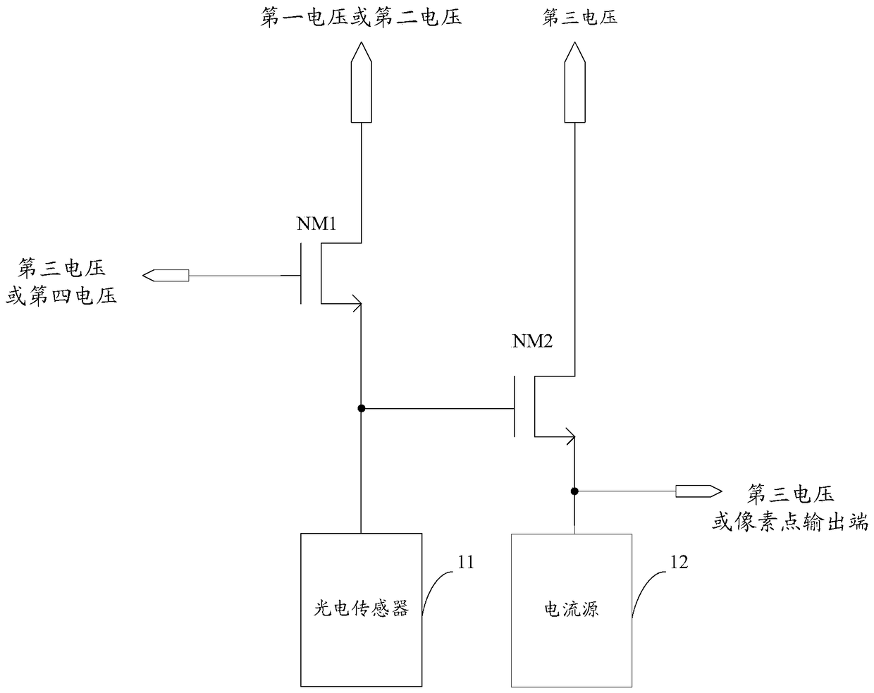
[0035] To solve this problem, the embodiment of the present invention connects the interstage capacitance of the pixel point structure that is not in the sampling state to the reference voltage, so that the reference voltage is connected to a capacitive load, and there is no need to introduce additional capacitance from the outside, thereby reducing the circuit area. Provides a stable reference voltage.

[0036] In order to make the above objects...


PUM


Abstract

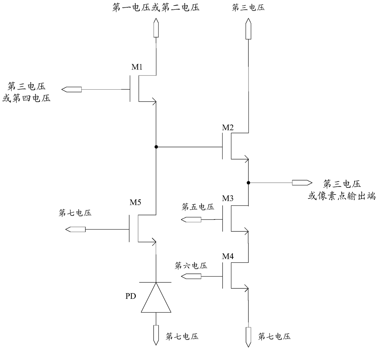
The invention discloses a pixel structure, an array and a control method of the pixel structure. The pixel structure comprises a first NMOS transistor, a second NMOS transistor, a photoelectric sensor and a current source. The drain electrode of the first NMOS transistor is selectively connected to a first voltage or a second voltage, the grid electrode of the first NMOS transistor is selectively connected to a third voltage or a fourth voltage, and the source electrode of the first NMOS transistor is connected to the grid electrode of the second NMOS transistor and the photoelectric sensor; the drain electrode of the second NMOS transistor is connected to the third voltage, the source electrode of the second NMOS transistor is connected to the current source, and the source electrode of the second NMOS transistor is selectively connected to the third voltage or the output end of a pixel. The pixel structure can be used for stabilizing the third voltage.

Description

technical field [0001] The invention relates to the field of electronics, in particular to a pixel structure, an array and a control method thereof. Background technique [0002] In order to obtain a stable reference voltage for an image processing chip with a pixel structure, it is usually necessary to connect a large capacitor as a load. However, by connecting a large capacitor outside the image processing chip to stabilize the reference voltage, a large capacitor needs to be added, which takes up a lot of space. The voltage stabilization effect is affected by the inductance generated by the chip package, and the stability of the reference voltage still needs to be improved. Contents of the invention [0003] The problem solved by the embodiments of the present invention is how to stabilize the reference voltage. [0004] To solve the above problems, an embodiment of the present invention provides a pixel structure, including: a first NMOS transistor, a second NMOS tran...

Claims


Application Information

Patent Timeline
Patent Type & Authority Patents(China)
IPC IPC(8): H04N5/374
Inventor 赵立新乔劲轩李敏兰
Owner GALAXYCORE SHANGHAI
Learn More