Printing ink hole plugging process method for circuit boards

A process method and circuit board technology, applied in the directions of printed circuits, printed circuit manufacturing, electrical components, etc., can solve the problems of poor ink plugging effect, etc., and achieve the effect of improving the effect, reducing the difficulty of alignment, and improving production efficiency.

Inactive Publication Date: 2015-04-01
SHENZHEN WUZHU TECH
View PDF10 Cites 9 Cited by
  • Summary
  • Abstract
  • Description
  • Claims
  • Application Information

AI Technical Summary

Problems solved by technology

[0005] In order to solve the technical problem of poor ink plugging effect in the above circuit board ink plug

Method used


Image

  • Printing ink hole plugging process method for circuit boards
  • Printing ink hole plugging process method for circuit boards
  • Printing ink hole plugging process method for circuit boards

Examples


Example Embodiment

[0050] The technical solutions in the embodiments of the present invention will be clearly and completely described below in conjunction with the accompanying drawings in the embodiments of the present invention. Obviously, the described embodiments are only a part of the embodiments of the present invention, rather than all the embodiments. Based on the embodiments of the present invention, all other embodiments obtained by those of ordinary skill in the art without creative work shall fall within the protection scope of the present invention.
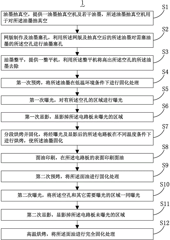
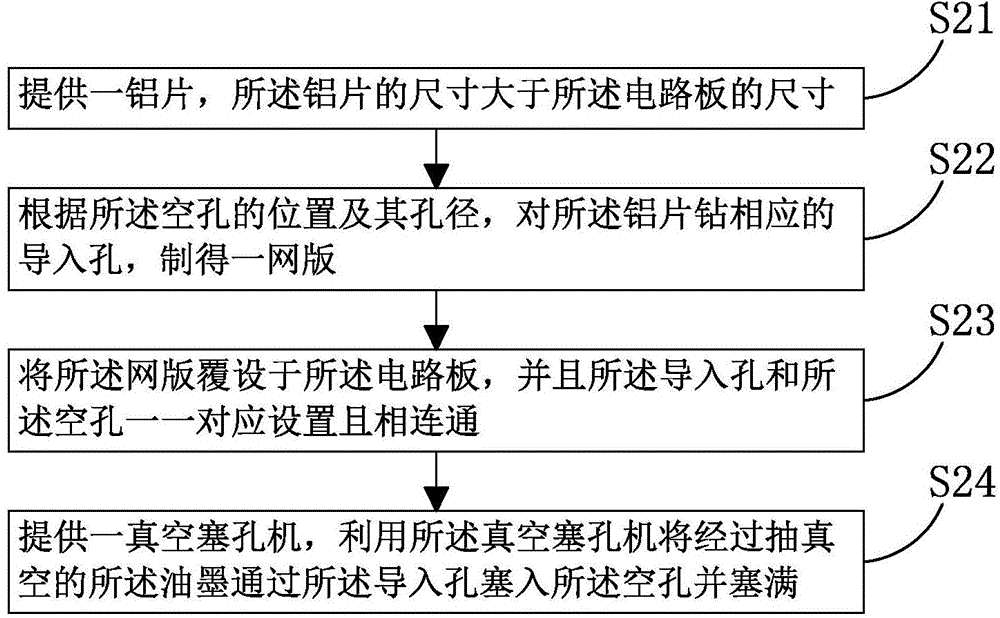
[0051] See figure 1 , Is the step flow chart of the circuit board ink plugging process method provided by the present invention. The method includes the following steps:

[0052] S1, the ink is vacuumed.

[0053] A circuit board, an ink vacuum machine and several inks are provided. The circuit board is a printed circuit board processed by drilling holes, electroless copper and pulse plating. The ink vacuum machine is used to vacuum the ink ...


PUM


Abstract

The invention provides a printing ink hole plugging process method for circuit boards. The printing ink hole plugging process method comprises the following steps: printing ink vacuumizing; screen printing plate production and printing ink hole plugging; printing ink leveling; pre-baking for the first time; exposing for the first time; developing for the first time; subsection baking and curing; surface oil printing; pre-baking for the second time; exposing for the second time; developing for the second time; high-temperature baking. The printing ink hole plugging process method reduces the probability that cracks exist in printing ink, improves the effect of printing ink hole plugging, and avoids the phenomenon that chemicals and humidity in the follow-up process can permeate into empty holes as the cracks exist in the cured printing ink.

Description

technical field [0001] The invention relates to the field of circuit board production, in particular to a process method for ink plugging of circuit boards. Background technique [0002] In today's society, the development of digital electronic products such as mobile phones, computers and cameras is advancing day by day, and is developing in the direction of lightness, thinness, shortness and smallness, and the requirements for the integration of electronic components are getting higher and higher. In particular, the demand for circuit boards is also increasing. In order to meet this demand, the manufacture of circuit boards is gradually developing towards the direction of highly integrated interconnection of line density. a very important step. [0003] The circuit board includes a variety of holes, except for component insertion holes, mounting holes, heat dissipation holes and test holes, most of the other holes do not need to be exposed. The ink plug hole can prevent ...

Claims


Application Information

Patent Timeline
IPC IPC(8): H05K3/40
CPCH05K3/40H05K3/4038H05K3/42
Inventor 徐学军
Owner SHENZHEN WUZHU TECH
Why Eureka
Try Eureka