Technique for local copper thinning and precision circuit making of printed circuit boards

A technology of printed circuit boards and process methods, which is applied in the direction of printed circuit manufacturing, printed circuits, electrical components, etc., and can solve the problem of not being able to meet the requirements of the thickness of copper on the hole and surface copper of the printed circuit board at the same time, the inconvenience of precision circuit manufacturing, and the production efficiency. Low-level problems, to achieve the effect of low equipment requirements, reduce production costs, and improve production efficiency

Inactive Publication Date: 2015-04-15
SHENZHEN WUZHU TECH
View PDF4 Cites 9 Cited by
  • Summary
  • Abstract
  • Description
  • Claims
  • Application Information

AI Technical Summary

Problems solved by technology

[0004] In order to solve the above-mentioned problems that the local copper thinning of the printed circuit board and the production of the precision circuit are complicated, the production efficiency is low, the requirements of the thickness of the copper on the hole and the thickness of the surface copper of the printed circuit board cannot be met at the same time, and it is not convenient for the manufacture of the precision circuit, the present invention Provides a process method for local copper thinning of printed circuit boards and precision circuit production, which has simple procedures, high production efficiency, can meet the thickness requirements of printed circuit board hole copper and surface copper, and is convenient for precision circuit manufacturing

Method used


Image

  • Technique for local copper thinning and precision circuit making of printed circuit boards
  • Technique for local copper thinning and precision circuit making of printed circuit boards

Examples


Embodiment Construction

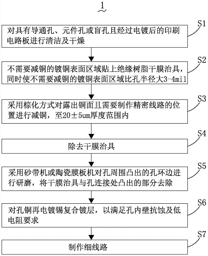
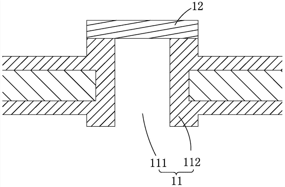
[0023] The following will clearly and completely describe the technical solutions in the embodiments of the present invention with reference to the accompanying drawings in the embodiments of the present invention. Obviously, the described embodiments are only some, not all, embodiments of the present invention. Based on the embodiments of the present invention, all other embodiments obtained by persons of ordinary skill in the art without making creative efforts belong to the protection scope of the present invention.

[0024] Please also refer to figure 1 and figure 2 ,in figure 1 It is a process flow diagram of a preferred scheme of the process method for locally thinning copper and precision circuit production of printed circuit boards provided by the present invention, figure 2 yes figure 1 A cross-sectional view of the processing structure during the copper reduction step of the process method for local thinning of copper and precision circuit manufacturing of the p...


PUM


Abstract

The invention provides a technique for local copper thinning and precision circuit making of printed circuit boards. The technique includes the following steps: adhering a dry film to a coppering surface region, with on need for copper reduction, of one printed circuit board with holes and subjected to electroplating; by adopting a brownification mode, subjecting the position exposing the copper surface and needing precision circuit making to copper thinning to the thickness range of 20+ / -5um; removing the dry film; removing the protruding parts of the joints of the dry film and the holes. According to the technique, the method of dry film isolating copper thinning is adopted, the thickness after copper plating of the holes is guaranteed, and the problem of under etching of the made precision circuit due to too thick surface copper is avoided.

Description

technical field [0001] The invention belongs to the field of processing and manufacturing of printed circuit boards, and in particular relates to a process method for locally thinning copper and precision circuit production of printed circuit boards. Background technique [0002] In the production process of printed circuit boards, the normal product requires a minimum copper thickness of 18um, but after actual electroplating, the minimum copper thickness of the hole is 20um, plus the thickness of the bottom copper 8um, the copper thickness of the hole after normal electroplating reaches 30±5um , far exceeding the ideal hole copper thickness of 20±5um for making 2mil lines. When it is necessary to manufacture precision circuits on the product, if the copper thickness on the circuit board surface is reduced, the copper thickness of the holes will also be reduced accordingly, which cannot meet the requirements of the copper thickness of the holes; however, the copper thickness...

Claims


Application Information

Patent Timeline
Patent Type & Authority Applications(China)
IPC IPC(8): H05K3/00
CPCH05K3/02H05K2203/14
Inventor 徐学军曾令雨赵南清
Owner SHENZHEN WUZHU TECH
Why Eureka
Try Eureka