Touch type liquid crystal display panel and touch type liquid crystal display device
A liquid crystal display panel and touch technology, which is applied in optics, instruments, electrical and digital data processing, etc., can solve the problems affecting the touch accuracy of the touch screen, and achieve the effect of improving the touch accuracy and increasing the sensing area.
- Summary
- Abstract
- Description
- Claims
- Application Information
AI Technical Summary
Problems solved by technology
Method used
Image
Examples
Embodiment 1
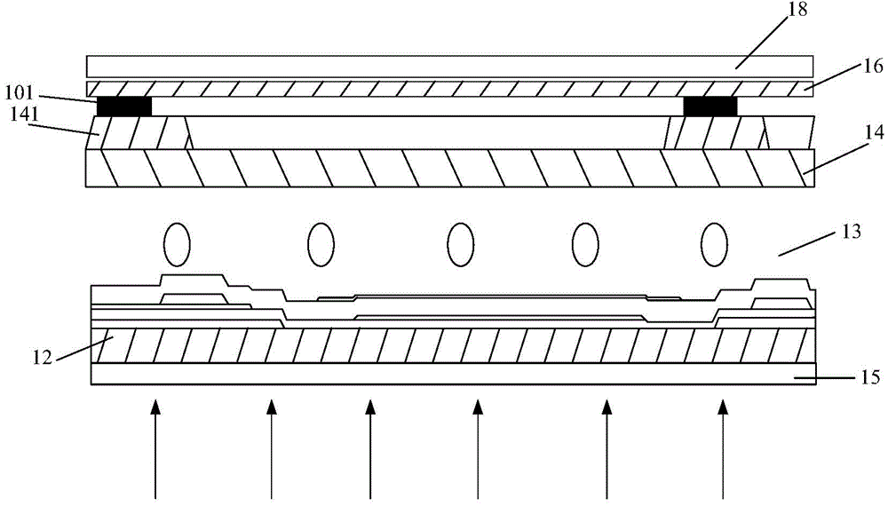
[0030] figure 2A schematic cross-sectional structure diagram of the touch-sensitive liquid crystal display panel in the first embodiment of the present invention is shown. Please refer to figure 2 , figure 2 The shown touch liquid crystal display panel includes: an array substrate 12, a color filter substrate 14, a lower polarizer 15 arranged below the array substrate 12, an upper polarizer 16 arranged above the color filter substrate 14, a set The cover plate 18 above the upper polarizer 16 and the liquid crystal layer 13 between the array substrate 12 and the color filter substrate 14 . The touch-sensitive liquid crystal display panel further includes a touch-control layer 101 , wherein, in this embodiment, the touch-control layer 101 is disposed on the color filter substrate 14 and faces one side of the upper polarizer 16 .
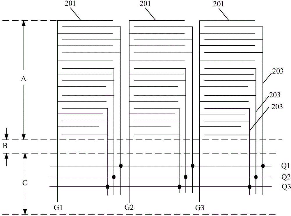
[0031] For the specific structure of the touch layer 101, please refer to image 3 , image 3 It is a schematic structural diagram of the touc...
Embodiment 2
[0049] Please refer to Figure 7 , Figure 7 A schematic cross-sectional structure diagram of the touch-sensitive liquid crystal display panel in the second embodiment of the present invention is shown. Figure 7 The structure shown is the same as figure 2 The touch-sensitive liquid crystal display panel shown is similar, and the difference is that a shielding layer 122 is arranged between the touch-control layer 101 and the upper polarizer 16, and the shielding layer 122 is made of opaque inorganic or organic materials, for example, The light reflected by the metal surface of the touch layer 101 is blocked to prevent light reflection on the touch layer 101 . Wherein, in the embodiment of the present invention, the wiring lines of the shielding layer 122 can be connected with Figure 4 The wiring lines of the sensing electrodes 201 and the driving electrodes 203 are exactly the same, and the width of the wiring lines of the shielding layer 122 is larger than the width of t...
PUM
 Abstract
Description
Claims
Application Information


