Design method for preventing upper MOS of VR from being broken down to burn up CPU

A design method, P12V technology, applied in the protection of under-voltage or no-voltage, data processing power supply, etc., can solve the problems of burning the CPU, burning the CPU, and using it for a long time.

Inactive Publication Date: 2015-04-29
LANGCHAO ELECTRONIC INFORMATION IND CO LTD
5 Cites 0 Cited by

AI-Extracted Technical Summary

Problems solved by technology

A problem that cannot be avoided whether it is a digital power supply or an analog power supply is: in a set of VR lines powered by multiple phases, once the upper MOS of one of the VR phases burns out, the 12V voltage on the motherboard will pass through the inductor in an instant. Directly connected to the CPU, causing the CPU to...

Abstract

The invention provides a design method for preventing an upper MOS of a VR from being broken down to burn up a CPU, and relates to the field of server DC power supply. PMOSs are added to two ends of an input capacitor; whether the upper MOS of the VR is broken down or not is judged by sensing voltage at two ends of the VR input capacitor; once the upper MOS is broken down, P12V is immediately pulled down, and short circuit protection of input voltage is triggered, so that power failure of the overall system is achieved; and the CPU is prevented from being burnt out.

Application Domain

Power supply for data processingArrangements responsive to undervoltage

Technology Topic

Short circuit protectionBurning out +6

Image

  • Design method for preventing upper MOS of VR from being broken down to burn up CPU
  • Design method for preventing upper MOS of VR from being broken down to burn up CPU

Examples

  • Experimental program(1)

Example Embodiment

[0011] Refer to the attached figure 1 , 2 , the present invention is further described by means of specific embodiments:
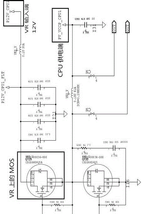
[0012] like figure 1 The schematic diagram of the VR principle before improvement is shown: it can be seen that if the upper MOS of VR is broken down, P12V_CPU0 will be directly connected to PV_VCCP_CPU0 through the upper MOS, and PV_VCCP_CPU0 is the power supply of the CPU, so once the upper MOS is hit wear, it is equivalent to the CPU directly connected to 12V, causing MOS to burn;
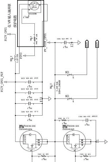
[0013] like figure 2 Shown is the improved design method (that is, proposed in this paper), which is realized by adding a PMOS at both ends of the input capacitor; in this way, when the upper MOS of VR breaks down, the voltage at both ends of the input capacitor will decrease, once The reduced voltage value is less than 3.3V (if the G electrode voltage is set higher, the trigger will be earlier), the VGS of the PMOS is less than 0, the PMOS will be turned on, and P12V_CPU0 will be directly connected to GND, and the voltage will be zero. At this time, the AC power supply will think that P12V_CPU0 is short-circuited to the ground, trigger the short-circuit protection, and turn off the power to prevent the CPU from being burned.
[0014] 1) According to the principle of VR design, it is calculated that when the 12V of the VR power supply input terminal is in normal operation of the VR, the fluctuation range of the voltage at both ends of the input capacitor determines the minimum voltage, which is generally greater than 10V;
[0015] 2) Combined with the output voltage value of VR (generally less than 2V), refer to the theoretical minimum value in step 1, and choose a reasonable level between the two, generally 3.3V is recommended;
[0016] 3) Connect a PMOS in parallel to the input capacitor terminal, the G pole of the PMOS is connected to the 3.3V voltage, the S pole is connected to the positive pole of the input capacitor, and the D pole is connected to the ground.
[0017] Through the above implementation steps, the design of the protection circuit to prevent the CPU from burning out can be completed.

PUM

no PUM

Description & Claims & Application Information

We can also present the details of the Description, Claims and Application information to help users get a comprehensive understanding of the technical details of the patent, such as background art, summary of invention, brief description of drawings, description of embodiments, and other original content. On the other hand, users can also determine the specific scope of protection of the technology through the list of claims; as well as understand the changes in the life cycle of the technology with the presentation of the patent timeline. Login to view more.
Why Eureka
Try Eureka