Touch display device

A touch display device and touch display technology, which are applied in the fields of optics, instruments, and electrical digital data processing, etc., can solve problems such as the reduction of touch accuracy and the distortion of touch sensing signal transmission, and achieve stable signal transmission effects and reduce Coupling capacitance and effects of reducing mutual interference

Active Publication Date: 2015-04-29
HONG FU JIN PRECISION IND (SHENZHEN) CO LTD +1
View PDF4 Cites 19 Cited by
  • Summary
  • Abstract
  • Description
  • Claims
  • Application Information

AI Technical Summary

Problems solved by technology

However, due to the coupling capacitance generated between the wires connected to the second sensing electrodes and the pins connected to the first sensing electrodes, the transmission of touch signals, especially touch sensing signals, is distorted under the influence of the coupling capacitance. , leading to a decrease in touch accuracy

Method used


Image

  • Touch display device
  • Touch display device
  • Touch display device

Examples


Embodiment Construction

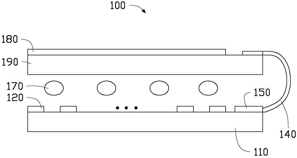
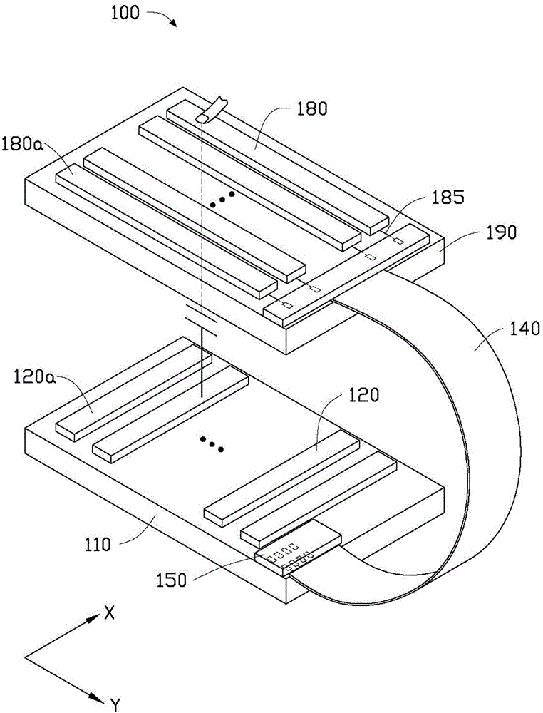
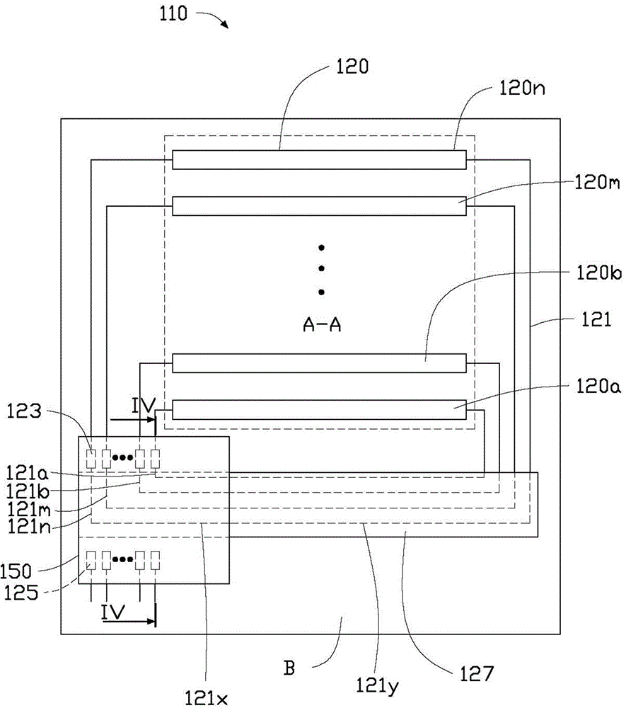
[0014] see figure 1 and figure 2 . In a specific implementation manner, the touch display device is specifically introduced by taking an in-cell touch type liquid crystal display device as an example. The touch display device 100 includes a first substrate 110, a second substrate 190, a liquid crystal layer 170, a plurality of first sensing electrodes 120, a plurality of second sensing electrodes 180, a touch sensing chip 150 and a flexible circuit board 140 . The first substrate 110 and the second substrate 190 clamp the liquid crystal layer 170 so that the liquid crystal layer 170 is sandwiched between the first substrate 110 and the second substrate 190 . The first sensing electrode 120 is disposed on a side of the first substrate 110 adjacent to the liquid crystal layer 170 . The second sensing electrode 180 is disposed on a side of the second substrate 190 , specifically, disposed on a side of the second substrate 190 away from the liquid crystal layer 170 . The tou...


PUM


Abstract

The invention relates to a touch display device. The touch display device comprises a first substrate and a second substrate which are oppositely arranged, first sensing electrodes and second sensing electrodes, wherein first pins transmit touch scanning signals, second pins transmit touch sensing signals, and the first substrate defines a touch display region and a non-touch display region; corresponding to the periphery of the non-touch display region, the first substrate is provided with the first pins, wires and the second pins; the first pins transmit the touch scanning signals and the second pins transmit the touch sensing signals; the wires are electrically connected with the corresponding sensing electrodes and the corresponding first pins, the second sensing electrodes are electrically connected with the corresponding second pins, the wires and the second pins are mutually insulated, a conductive layer is arranged at a part, close to the second pins, of the wires, and is located in a layer between the part, close to the second pins, of the wires and the second pins, and the conductive layer is grounded or is in direct electric signal connection with a constant potential. The touch display device is relatively high in touch precision.

Description

technical field [0001] The invention relates to a touch display device. Background technique [0002] A touch display device, such as an embedded touch liquid crystal display device, includes a color filter substrate, a thin film transistor array substrate, a liquid crystal layer sandwiched between the color filter substrate and the thin film transistor array substrate, The first sensing electrode for generating a corresponding touch sensing signal and the second sensing electrode for receiving the touch scanning signal are used for sensing the touch scanning signal. The first sensing electrodes are usually disposed on one side of the color filter substrate. The second sensing electrode is disposed on a side of the thin film transistor array substrate adjacent to the liquid crystal layer. The first sensing electrodes are connected to the corresponding pins of the touch sensing chip through the flexible circuit board and the pins of the non-display area on the thin film tra...

Claims


Application Information

Patent Timeline
Patent Type & Authority Applications(China)
IPC IPC(8): G06F3/041G02F1/1333
CPCG02F1/13338G02F1/1345G06F3/0412G06F3/044G06F2203/04111
Inventor 黄鸿运刘家麟陈维成
Owner HONG FU JIN PRECISION IND (SHENZHEN) CO LTD
Why Eureka
Try Eureka