Method of fabrication of MIMCAP and resistor at same level

a technology of resistor and mimcap, which is applied in the manufacture of capacitors, variable capacitors, fixed capacitors, etc., can solve the problems of adding to the interconnection delay of typical circuits, adding to the interconnection delay of oscillator circuits, and complex wiring, so as to reduce parasitics, reduce design complexity, and use efficient existing wiring levels

Inactive Publication Date: 2006-04-04
GLOBALFOUNDRIES US INC
View PDF8 Cites 18 Cited by
  • Summary
  • Abstract
  • Description
  • Claims
  • Application Information

AI Technical Summary

Benefits of technology

[0007]The present invention provides a single level integration process for the fabrication of a MIMCAP and a thin film TaN (tantalum nitride) resistor which allows both a BEOL (back-end-of-line) capacitor and a thin film TaN resistor to be fabricated at the same level. The integration process allows the two devices to be wired at the lowest metal level (M1), which had previously not been possible with prior art BEOL passive circuits. Circuit designers can now wire to the TaN thin film resistor at the lowest metal level, which reduces parasitics and allows more efficient usage of the existing wiring levels. The present invention reduces the design complexity and enhances the performance of the resultant circuits.
[0008]The number of processing steps is reduced using this fabrication process. The integration challenges in the prior art process (e.g. vias landing on the resistor and the capacitor) are eliminated. The process sequence of the present invention reduces cost, enhances performance and improves usability of the resultant circuits.
[0009]The wiring path to the thin film TaN resistor is reduced and simplified using the fabrication process sequence, which reduces the interconnect delay and coupling capacitance in the circuit, improving the circuit performance for both digital and analog applications. The integration scheme places the thin film resistor on top of the CA (contact metal) level, and the thin film resistor is interconnected through the M1 level which provides a shorter interconnect path than current prior art integration schemes.
[0010]The thermal resistance of the thin film resistor is lower than the thermal resistance of a prior art resistor produced by current prior art processes because of the proximity of the circuit elements to the substrate and the intimate contact thereof with metal lines, rather than by contact through vias as in the prior art. The low thermal resistance reduces the temperature coefficient of the thin film resistor, allowing circuit designers to possibly use a BEOL resistor as a precision resistor device, which has not been possible with current prior art processes.
[0011]The thermal resistance of the thin film resistor is improved due to the better heat dissipation through the silicon substrate, as the thin film resistor is closer to the silicon substrate which functions as a heat sink. Because of the proximity of the TaN resistor to the bulk silicon substrate, the thermal resistance (Rth) of the TaN resistor is 16–23% (15–21%?) less than a TaN resistor on BPSA implemented in the current prior art 8HP module, and is 60–70% less than the TaN resistor on STI implemented in the current prior art 8HP module. A temperature rise of a thin film resistor may adversely impact upon the reliability of the circuit and has been a concern. The reduction of thermal resistance and temperature rise of the thin film resistor produced by the process of the present invention improves the reliability of the circuit.
[0012]The wiring path to the thin film resistor is shortened using the process of the present invention, which reduces the interconnect delay and coupling capacitance in the circuit to improve circuit performance. The wiring path for a thin film resistor using the current prior art integration scheme CA-->M1--->V1--->M1-->V1-->K1 and back in the reverse order to CA. In contrast thereto, the wiring path for a thin film resistor using the process of the present invention is a serial connection comprising CA--->M1-->K1 and back in the reverse order to CA.

Problems solved by technology

Because the thin film resistors are so far away from the transistor devices, the wiring is often quite complicated and lengthy, adding to the interconnect delay of typical circuits of any type such as amplifier circuits and oscillator circuits.

Method used


Image

  • Method of fabrication of MIMCAP and resistor at same level
  • Method of fabrication of MIMCAP and resistor at same level
  • Method of fabrication of MIMCAP and resistor at same level

Examples


Embodiment Construction

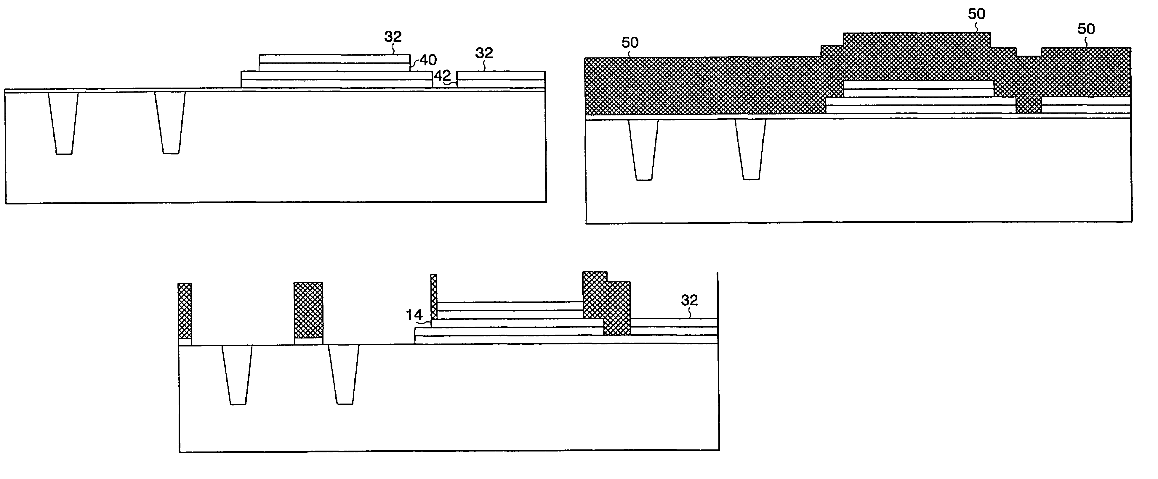
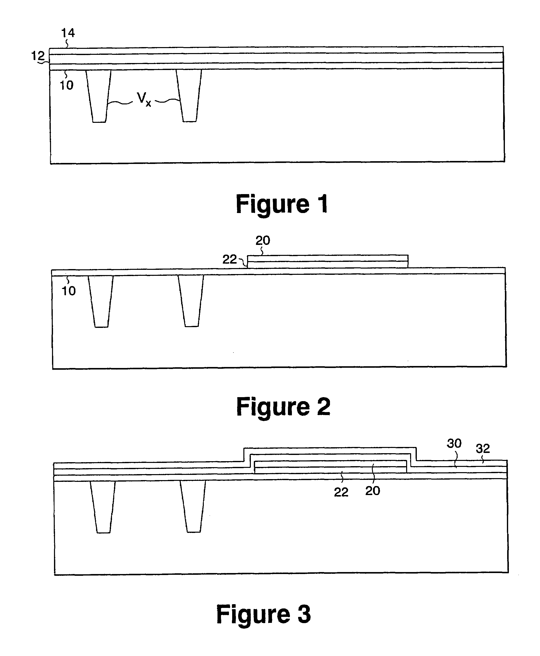
[0042]FIGS. 1–10 illustrate the sequential steps of a method for fabricating a MIMCAP (a capacitor (CAP) formed by successive layers of metal, insulator, metal (MIM)) and a thin film resistor at the same level.

[0043]FIG. 1 illustrates the structure, which could be at any via level and preferably at the lowest metal level (M1), after steps of depositing a 300A layer 10 of oxide insulation, then depositing a layer of metal 12 such as TaN on top of the layer of oxide insulation to form the bottom electrode of the capacitor, then depositing a layer of dielectric 14 such as tantalum pentoxide, silicon nitride or silicon dioxide on top of the layer of metal to form the dielectric of the capacitor. Vias Vx are also shown as being representative of a typical circuit.

[0044]FIG. 2 illustrates the structure after steps of lithographic patterning and etching the dielectric 20 and the bottom electrode 22 of the capacitor.

[0045]FIG. 3 illustrates the structure after steps of depositing a layer of...


PUM

PropertyMeasurementUnit
structureaaaaaaaaaa
coupling capacitanceaaaaaaaaaa
thermal resistanceaaaaaaaaaa

Abstract

A method is disclosed of fabricating a MIMCAP (a capacitor (CAP) formed by successive layers of metal, insulator, metal (MIM)) and a thin film resistor at the same level. A method is also disclosed of fabricating a MIMCAP and a thin film resistor at the same level, and a novel integration scheme for BEOL (back-end-of-line processing) thin film resistors which positions them closer to FEOL (front-end-of-line processing) devices.

Description

BACKGROUND OF THE INVENTION[0001]1. Field of the Invention[0002]The present invention relates generally to a method of fabricating a MIMCAP (a capacitor (CAP) formed by successive layers of metal, insulator, metal (MIM)) and a thin film resistor at the same level. The subject invention also pertains to a method of fabricating a MIMCAP and thin film resistor at same level, and a novel integration scheme for BEOL (back-end-of-line processing) thin film resistors which positions them closer to FEOL (front-end-of-line processing) devices.[0003]2. Discussion of the Prior Art[0004]In the prior art, thin film resistors are currently incorporated in the BEOL (back-end-of-line processing) levels, typically between the MX (M1 / MT) metal levels or at the thick interconnect level, wherein MX designates any metal layer. Because the thin film resistors are so far away from the transistor devices, the wiring is often quite complicated and lengthy, adding to the interconnect delay of typical circuit...

Claims


Application Information

Patent Timeline
Patent Type & Authority Patents(United States)
IPC IPC(8): H01L21/302H01L21/768H01L21/02H01L21/3205H01L21/822H01L23/52H01L23/522H01L27/04H01L27/08
CPCH01L23/5223H01L27/0802H01L27/0805H01L28/20H01L28/40Y10T29/49155H01L2924/0002Y10S438/97Y10T29/49082H01L2924/00
Inventor CHINTHAKINDI, ANIL K.JENG, SHWU-JENLOFARO, MICHAEL F.SCHNABEL, CHRISTOPHER M.STEIN, KENNETH J.
Owner GLOBALFOUNDRIES US INC
Why Eureka
Try Eureka