Stacked synchronous buck converter having chip embedded in outside recess of leadframe

a synchronous buck converter and chip technology, applied in semiconductor devices, semiconductor/solid-state device details, electrical apparatus, etc., can solve the problems of significant parasitic inductance into the power circuit, excessive and significant risk of wire sweep and electrical shortening, so as to shorten the length of bonding wires and save the height of the stacking system, the effect of saving board real esta

Active Publication Date: 2015-11-10
TEXAS INSTR INC
View PDF5 Cites 9 Cited by
  • Summary
  • Abstract
  • Description
  • Claims
  • Application Information

AI Technical Summary

Benefits of technology

[0006]Applicants realized that that the ongoing trend of employing DC-DC converters in new applications, such as automotive products, accelerates the long-standing drive towards miniaturization, lower power, and reduced cost. Symptoms of this trend are the pushes for reducing the height of converters and the reduction of board real estate consumed of the converter.
[0007]Applicants further realized that a step function improvement in reducing the height of stacked converters and shrinking the board area consumed could be achieved when an element of the stacked converter could be eliminated without eliminating the function of that element. For DC-DC converters with a vertically stacked assembly of chips and clips on a leadframe, applicants found a way of eliminating a clip while retaining its function, when they discovered a method of re-arranging the overall assembly of chips, clips and leadframe together with re-arranging the electrical current flow. As unexpected side benefits, it turned out that the new hierarchy reduces parasitics of the converter, increases its speed, and simplifies the assembly flow.
[0010]Compared to conventional power supply systems, the invention saves board real estate by fully integrating the driver-and-controller chip into the vertical stack, and by shortening the bonding wire length to a value save against wire sweep The invention further saves height of the stacked system by embedding one FET chip into the partially thinned leadframe pad. This feature allows the elimination of the conventional second clip without abandoning its function. As a consequence, the resistance of the second clip is eliminated, thus improving the speed of the converter and reducing its parasitic loss; in addition, the assembly flow is shortened, reducing the manufacturing cost.

Problems solved by technology

The electrical connections from the chips to the leads may be provided by bonding wires, which introduce, due to their lengths and resistances, significant parasitic inductance into the power circuit.
Independent of the physical size, the sync FET chip needs a larger active area than the active area of the control FET chip, due to considerations of duty cycle and conduction loss.
In other known converters with smaller chips, the driver chip may be placed in top of the second clip to sane board area; for these converters, however, the bonding wires have to be excessively long with significant risk of wire sweep and electrical short during the encapsulation process.

Method used


Image

  • Stacked synchronous buck converter having chip embedded in outside recess of leadframe
  • Stacked synchronous buck converter having chip embedded in outside recess of leadframe
  • Stacked synchronous buck converter having chip embedded in outside recess of leadframe

Examples


Embodiment Construction

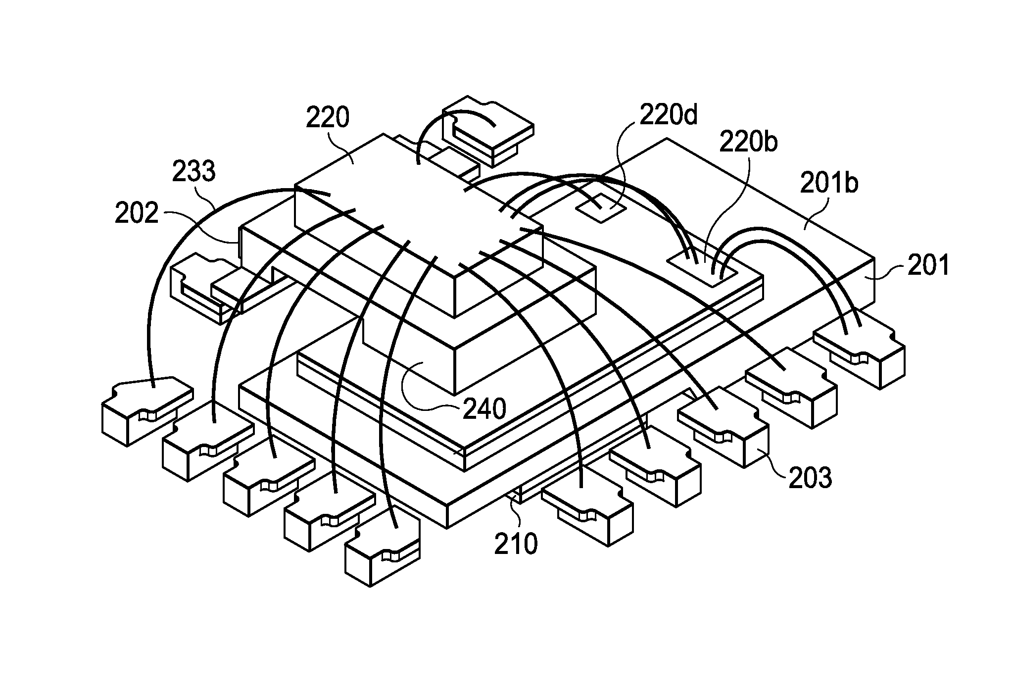
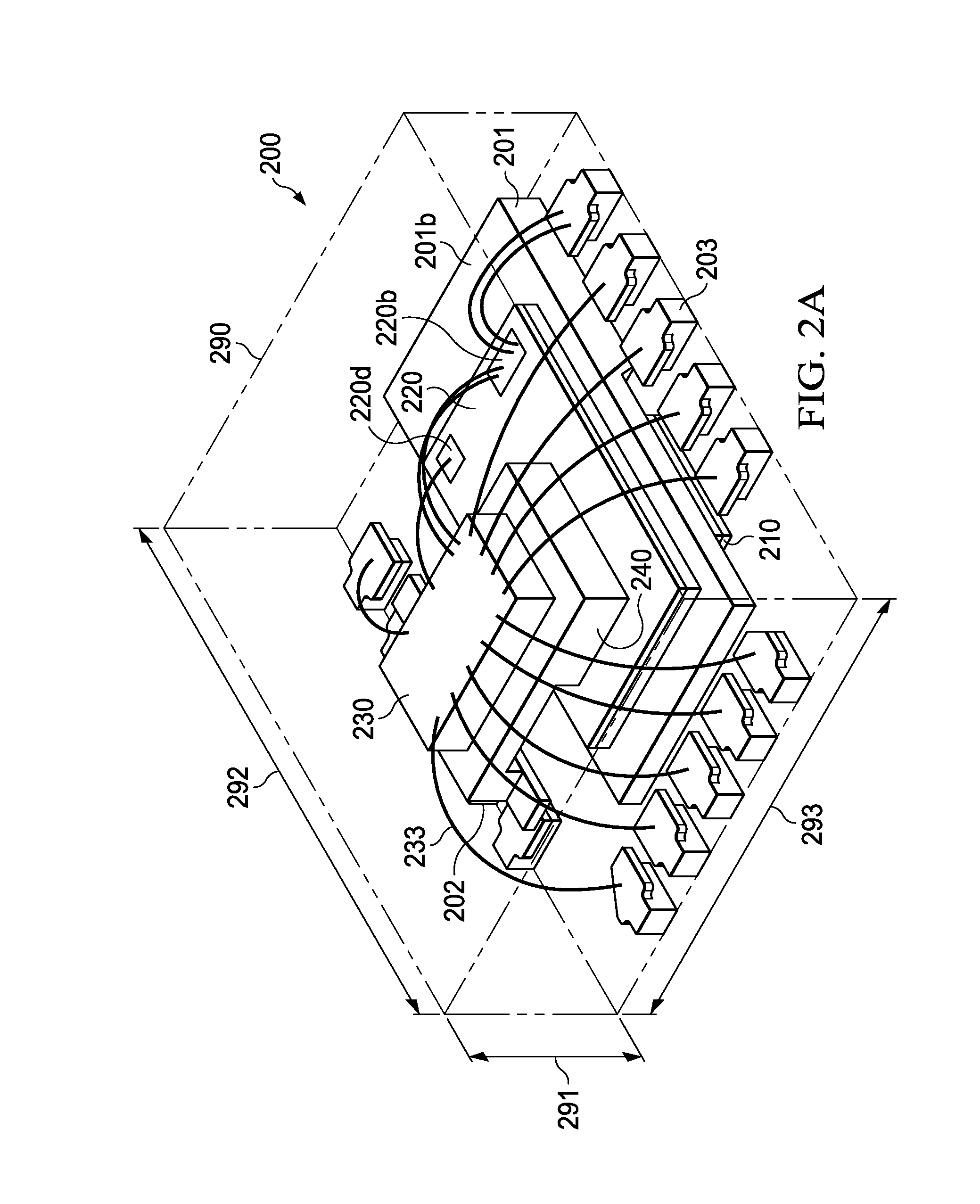
[0028]FIGS. 2A and 2B illustrate perspective views of a power supply module generally designated 200 as an exemplary embodiment of the invention, FIG. 2A as a top view, FIG. 2B as a bottom view. For explanatory reasons, module 200 is shown with a transparent encapsulation 290. Preferred actual encapsulation uses a black-colored epoxy formulation for a transfer molding technology. The exemplary module of FIGS. 2A and 2B has a thickness 291 of 1.0 mm and a square-shaped footprint with a module length 292 of 3.0 mm and a width 293 of 3.0 mm. Other pads may be rectangular.

[0029]Visible through the transparent encapsulation is a metal leadframe generally suitable for Quad Flat No-Lead (QFN) and Small Outline No-Lead (SON) type modules. The leadframe includes a rectangular pad 201 and a plurality of leads 202 and 203. The pad surface visible in FIG. 2B is the first surface 201a, the pad surface visible in FIG. 2A is the second surface 201b. The leadframe is preferably made of copper or a ...


PUM


Abstract

A power supply system (200) has a QFN leadframe with leads and a pad (201, switch node terminal); a pad surface having a portion recessed with a depth (270) and an outline suitable for attaching a semiconductor chip. A first FET chip (220) is vertically stacked to the opposite pad surface. A clip (240) is vertically stacked on the first FET chip and tied to a lead (202, grounded output terminal). A second FET chip (210) has its source terminal attached to the recessed portion and its drain (210a, input terminal) and gate (210b) terminals co-planar with the un-recessed portion. A driver-and-controller chip (230) is attached to the clip. Packaging compound (290) encapsulates the parts but leaves a pad surface and the drain and gate terminals of the second FET chip un-encapsulated.

Description

FIELD[0001]Embodiments of the invention are related in general to the field of semiconductor devices and processes, and more specifically to the structure and fabrication method of packaged synchronous Buck converters, which have stacked chips and clips and also a chip embedded outside the package in a pre-coined recess of the leadframe.DESCRIPTION OF RELATED ART[0002]Among the popular families of power supply circuits are the power switching devices for converting on DC voltage to another DC voltage. Particularly suitable for the emerging power delivery requirements are the Power Blocks with two power MOS field effect transistors (FETs) connected in series and coupled together by a common switch node; such assembly is also called a half bridge. When a regulating driver and controller is added, the assembly is referred to as Power Stage or, more commonly, as Synchronous Buck Converter. In the synchronous Buck converter, the control FET chip, also called the high-side switch, is conn...

Claims


Application Information

Patent Timeline
Patent Type & Authority Patents(United States)
IPC IPC(8): H01L23/495H01L21/56H01L25/00H01L23/00H01L25/16H01L23/31H01L25/065
CPCH01L23/49575H01L21/56H01L23/3107H01L23/49503H01L23/49562H01L24/49H01L24/83H01L24/85H01L25/165H01L25/50H01L23/49524H01L25/0657H01L2224/32145H01L2224/32147H01L2224/32148H01L2224/48091H01L2224/48106H01L2224/48247H01L2224/49171H01L2224/8385H01L2224/83801H01L2224/83851H01L2924/1306H01L2924/1425H01L2924/1426H01L2924/181H01L23/49548H01L2924/00014H01L2924/13091H01L24/40H01L2224/40245H01L2224/48145H01L2224/4103H01L2224/92242H01L2224/84447H01L2224/84444H01L2224/84439H01L2224/40499H01L24/27H01L24/29H01L24/32H01L24/33H01L24/37H01L24/41H01L24/48H01L24/73H01L24/84H01L24/92H01L2224/27312H01L2224/291H01L2224/2919H01L2224/2929H01L2224/293H01L2224/32245H01L2224/33181H01L2224/37147H01L2224/4911H01L2224/49111H01L2224/73221H01L2224/73263H01L2224/73265H01L2224/83191H01L2224/83192H01L2224/83439H01L2224/83444H01L2224/83455H01L2224/83464H01L2224/83815H01L2224/83862H01L2224/85439H01L2224/85444H01L2224/85455H01L2224/85464H01L2224/92147H01L2224/9221H01L2224/92247H01L2224/29294H01L2224/48111H01L2224/8391H01L2224/73271H01L2224/84464H01L2224/92157H01L2224/84455H01L2224/92252H01L2224/84815H01L2224/8491H01L2924/14252H01L2224/37013H01L2224/41051H01L2224/40095H01L2224/84801H01L2224/45015H01L2924/20752H01L2224/45099H01L2924/00H01L2924/00012H01L2924/014H01L2924/0665H01L2924/07811H01L2924/07812H01L2224/83447H01L2224/83H01L2224/84H01L2224/85H01L2224/27H01L23/49541H01L2225/0651
Inventor LOPEZ, OSVALDO JORGENOQUIL, JOHATHAN A.
Owner TEXAS INSTR INC
Why Eureka
Try Eureka