Semi-suspension graphene field effect transistor preparation method

A field-effect transistor and suspended graphite technology, which is applied in semiconductor/solid-state device manufacturing, semiconductor devices, electrical components, etc., can solve the problem of reducing carrier mobility, damage and contamination in graphene, and limiting the high frequency of graphene transistors Performance and other issues, to avoid damage and contamination, reduce parasitic, and ensure the integrity of the crystal

Active Publication Date: 2015-11-11
THE 13TH RES INST OF CHINA ELECTRONICS TECH GRP CORP
View PDF4 Cites 10 Cited by
  • Summary
  • Abstract
  • Description
  • Claims
  • Application Information

AI Technical Summary

Problems solved by technology

Experiments have found that transferred CVD graphene is susceptible to damage and contamination, and the interface scattering generated by the direct contact between the substrate and graphene will seriously reduce the mobility of carriers in graphene, which limits the high frequency of graphene transistors. performance

Method used


Image

  • Semi-suspension graphene field effect transistor preparation method
  • Semi-suspension graphene field effect transistor preparation method
  • Semi-suspension graphene field effect transistor preparation method

Examples


preparation example Construction

[0036] Overall, the present invention discloses a method for preparing a semi-suspended graphene field-effect transistor, the method comprising the steps of:

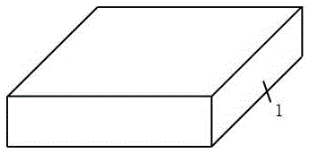
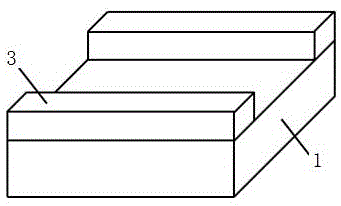
[0037] 1) On Substrate 1 (eg figure 1 As shown), the upper surface of the photoresist is coated, and the photolithography process is carried out to form the first photoresist pattern 3, such as figure 2 shown; the substrate can be SiO 2 , Si, SiC, sapphire, diamond, glass, mica or ceramics and other solid insulating substrates.

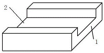
[0038] 2) Using the first photoresist pattern 3 on the upper surface of the substrate 1 as a mask, the substrate 1 is etched to form a substrate structure with grooves 2, such as image 3 Shown; groove size: depth 1 nm-100 μm, length and width 10 nm-100 μm.

[0039] 3) Metal-based graphene4 was prepared by chemical vapor deposition, such as Figure 4 As shown, the metal-based graphene is copper foil-based graphene or nickel foil-based graphene.

[0040] 4) Deposit a metal layer 5 on the u...

Embodiment 1

[0048] 1) First, prepare the substrate, the substrate used is insulating Si, such as figure 1 .

[0049] 2) Coating photoresist on the substrate, performing a photolithography process, and forming a photoresist pattern, such as figure 2 shown.

[0050] 3) Using the photoresist pattern formed in step 2) as a mask, the substrate is etched to a depth of 1 μm. After the etching is completed, the photoresist is removed to form a image 3 The substrate structure shown.

[0051] 4) Prepare metal-based graphene prepared by CVD method, the material used is copper foil-based graphene, such as Figure 4 shown.

[0052] 5) Using an electron beam evaporation station, in Figure 4 A layer of Au is deposited on the graphene of the shown structure with a thickness of 200nm to form a Figure 5 structure shown.

[0053] 6) put Figure 5 The shown graphene assembly with a bimetallic sandwich structure placed in a concentration of 1mol / L FeCl 3 In the etching solution, the Cu attached t...

Embodiment 2

[0059] 1) First, prepare the substrate, the substrate used is diamond, such as figure 1 .

[0060] 2) Coating photoresist on the diamond substrate, performing a photolithography process, and forming a photoresist pattern, such as figure 2 .

[0061] 3) Using the photoresist pattern formed in step 2) as a mask, the substrate is etched to a depth of 2 μm. After the etching is completed, the photoresist is removed to form a image 3 The substrate structure shown.

[0062] 4) Prepare metal-based graphene prepared by CVD method, the material used is copper foil-based graphene, such as Figure 4 shown.

[0063] 5) Using an electron beam evaporation station, in Figure 4 Deposit a layer of Pb on the graphene of the shown structure, the thickness is 100nm, forms as Figure 5 structure shown.

[0064] 6) put Figure 5 The shown graphene assembly with a bimetallic sandwich structure placed in a concentration of 1mol / L FeCl 3 In the etching solution, the Cu attached to the grap...


PUM

PropertyMeasurementUnit
depthaaaaaaaaaa
widthaaaaaaaaaa
widthaaaaaaaaaa

Abstract

The invention discloses a semi-suspension graphene field effect transistor preparation method, and relates to the technical field of transistors. The semi-suspension graphene field effect transistor preparation method comprises the following steps that photoresist is coated on a substrate so that a photoresist pattern is formed; the photoresist pattern acts as a mask film to form a substrate structure with grooves; metal-based graphene is prepared via a chemical vapor deposition method; a metal layer is deposited on the upper surface of metal-based graphene; the metal base below metal-based graphene is corroded so that a graphene assembly is formed; the graphene assembly is transferred to the substrate structure with the grooves; a second photoresist pattern is formed on the upper surface of the metal layer; the second photoresist pattern acts as the mask film to form a drain electrode and a source electrode; and the second photoresist pattern acts as the mask film, and gate metal is deposited on an insulating medium. Damage and contamination of graphene can be avoided by the method. Interface scattering of the substrate is reduced by separation of graphene and the substrate so that high mobility of carriers in graphene is realized and high-frequency performance of a graphene transistor is enhanced.

Description

technical field [0001] The invention relates to the technical field of transistors, in particular to a method for preparing a semi-suspended graphene field-effect transistor. Background technique [0002] In the field of integrated circuits, according to Moore's Law, the number of transistors in a chip will double every 18 months. With the improvement of chip integration, the feature size of transistors based on silicon materials is continuously shrinking, and is gradually approaching its physical limit. In order to maintain the continuous development of integrated circuits, it is necessary to introduce new technologies and materials. New materials are always the foundation and focus of the modern electronics industry. Among them, graphene, as a new generation of semiconductor materials, has great development potential and is expected to replace silicon and be used in electronic devices. middle. [0003] Graphene is a hexagonal honeycomb two-dimensional crystal composed of...

Claims


Application Information

Patent Timeline
Patent Type & Authority Applications(China)
IPC IPC(8): H01L21/336
CPCH01L29/66477
Inventor 冯志红何泽召李佳蔚翠刘庆彬芦伟立
Owner THE 13TH RES INST OF CHINA ELECTRONICS TECH GRP CORP
Why Eureka
Try Eureka