Method and apparatus for switching audio and data signals through a single terminal

a single terminal and audio and data technology, applied in electronic switching, pulse automatic control, pulse technique, etc., can solve the problems of high cost and substantial capacitive load at the common terminal, distortion of audio signals, etc., to reduce the occupancy area of semiconductor circuits, minimize parasitic capacitance, and facilitate switching

Active Publication Date: 2009-01-27
INTERSIL INC
View PDF3 Cites 10 Cited by
  • Summary
  • Abstract
  • Description
  • Claims
  • Application Information

AI Technical Summary

Benefits of technology

[0010]It should be noted that in certain applications where the digital data signal is of reduced amplitude, a single MOSFET may be used to switch the data signals instead of a CMOS-based switch, thereby saving additional area and minimizing parasitic capacitance. This combination of a single MOSFET-switch for the audio signal path and a CMOS-based or MOS-based switching circuit for the digital data path implements a single pole, double throw (SPDT) switching function, with the auxiliary MOSFET switching circuit being biased either ON or OFF, so that it operates as an application specific switch. This enables both switching circuits to be tailored for the applications in which they are to perform. For example, the auxiliary switching circuit may be employed to pass audio signals to a speaker load with minimal distortion, while the CMOS-based or MOS-based circuit is used to pass high speed data signals with minimal loss of speed.
[0020]The multi signal-switching circuit architecture of the invention is particularly useful in small hand-held devices having audio signal communication capability, such as, but not limited to, MP3 players, cell phones, digital cameras, and personal digital assistants (PDAs), where small size, reduced cost, and high performance have become standard requirements. The invention allows the use of a single mechanical connector (in place of multiple connectors of a conventional device) for passing high quality data signals (which may include audio information or a combination of audio and video for playback) into the device, thereby reducing size, weight and cost. Also, the reduction of parasitics in the digital signal path improves the data rate that can be used for transferring data into or out of the device, thereby reducing data transfer time and allowing larger memory sizes.

Problems solved by technology

Unfortunately, such a replicated switch-based architecture has a number of inherent drawbacks.
This results in high cost and substantial capacitive loading at the common terminal.
A second shortcoming is the fact that the gate-to-source voltage of the audio circuit's switching MOSFETs varies with the analog (audio) signal, which produces modulation of the ON-resistance of the switching MOSFETs, thereby causing distortion of the audio signal.

Method used


Image

  • Method and apparatus for switching audio and data signals through a single terminal
  • Method and apparatus for switching audio and data signals through a single terminal
  • Method and apparatus for switching audio and data signals through a single terminal

Examples


first embodiment

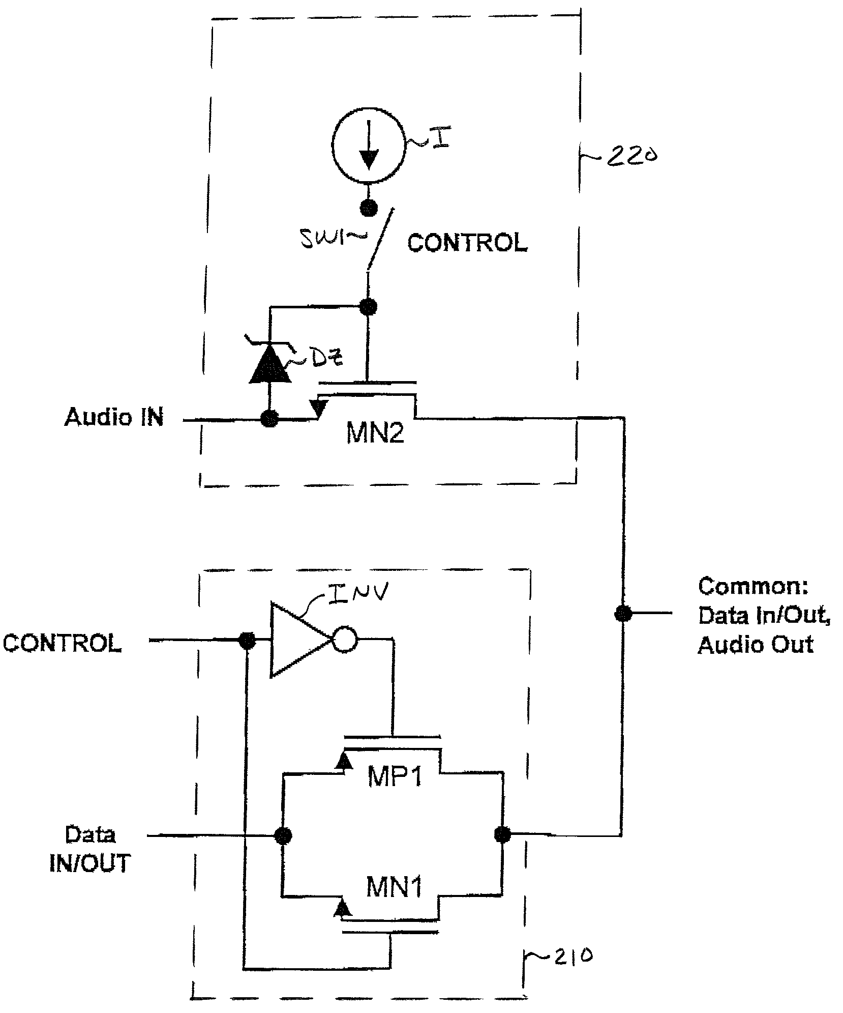
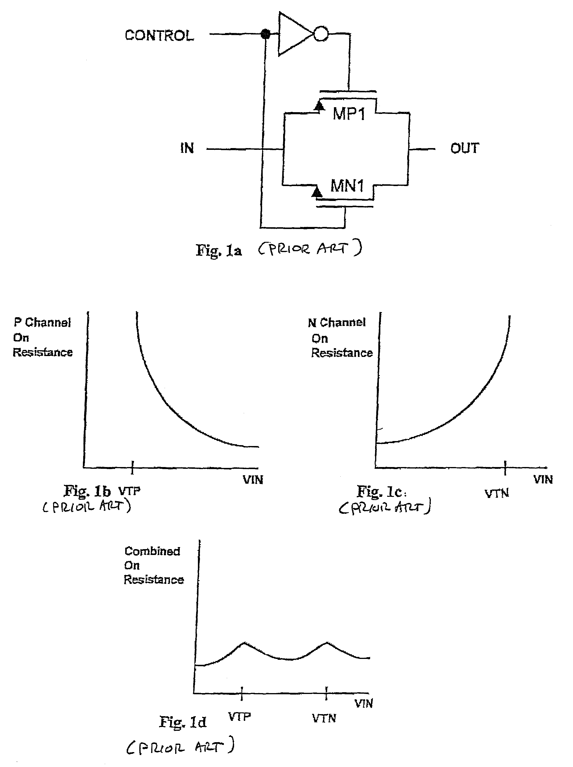
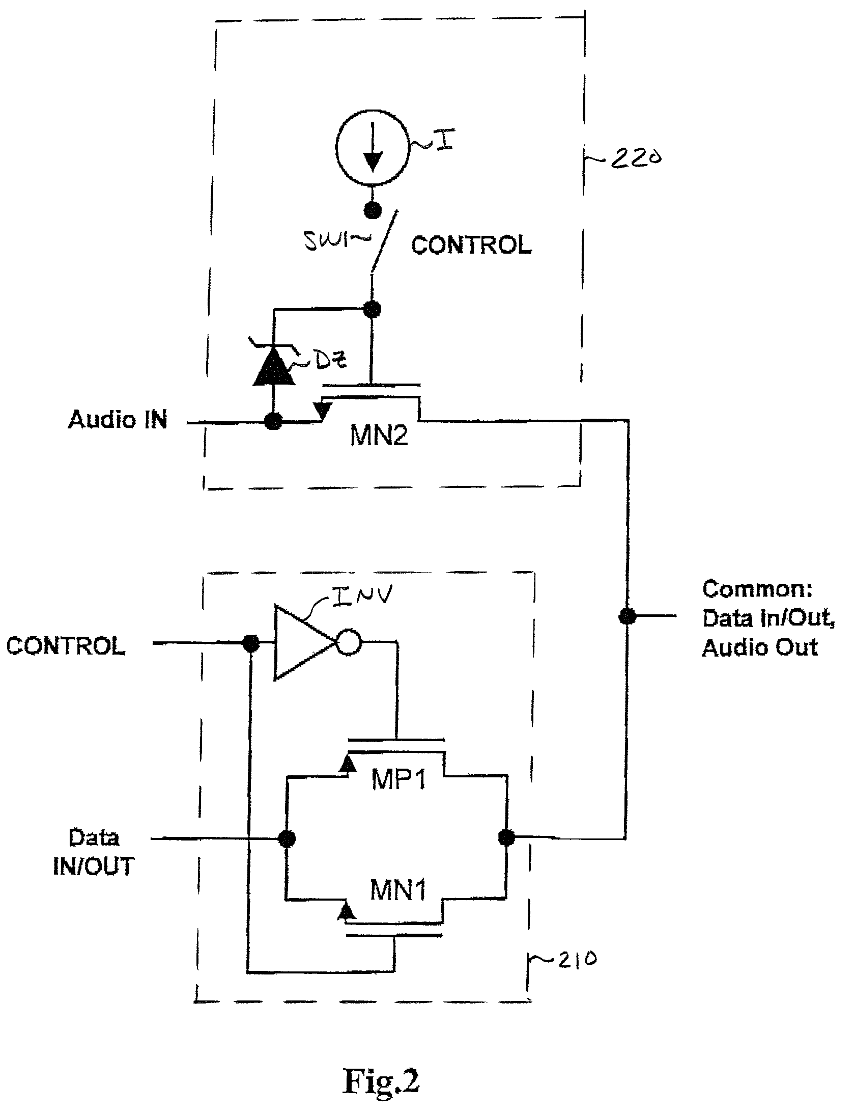
[0030]Attention is now directed to FIG. 2, which schematically illustrates the multi-signal SPDT switching circuit of the present invention, as a combination of a high speed data signal switch 210, which may be implemented by the CMOS switching circuit of FIG. 1a, and an auxiliary analog (e.g., audio) signal switch 220, which is implemented by a single NMOS transistor MN2, having its source-drain path coupled between an analog / audio input terminal / port ‘Audio In’ and the signalling interface terminal / port ‘Common’, through which analog / audio output signals, as well as data input and output signals, are coupled. As noted previously, porting both analog / audio and data signals to the same signalling interface terminal ‘Common’ allows the use of a single mechanical connector to pass high quality data signals into the device, thereby reducing size, weight and cost.

[0031]In the first embodiment of the invention shown in FIG. 2, the single analog / audio signal switching N-channel MOSFET MN2...

second embodiment

[0033]FIG. 3 schematically illustrates the multi-signal SPDT switching circuit of the invention, wherein the gate-to-source voltage-clamping Zener diode Dz of the audio signal switch 220 of the embodiment of FIG. 2 is replaced by a gate-to-source coupling resistor R. The multi-signal switching circuit of FIG. 3 is otherwise the same as that of FIG. 2. The injection of a constant bias current from the constant current source I through the gate-to-source coupling resistor R for the ON state of the switching MOSFET MN2 sets the gate-to-source bias voltage VGS of MOSFET MN2 at a constant value, corresponding to the product of the coupling resistance R and the value of the constant current I. This allows the multi-signal switching circuit of FIG. 3 to offer the same advantages as the implementation of FIG. 2, over using two of the conventional signal CMOS-based analog signal switching circuits of FIG. 1a for respective audio and digital signaling paths to implement the desired SPDT switc...

third embodiment

[0034]FIG. 4 schematically illustrates the multi-signal SPDT switching circuit of the invention, wherein the Zener diode Dz and the resistor R of the audio signal switch 220 of the respective multi-signal switching circuits of the embodiments of FIGS. 2 and 3 are replaced by a gate-to-source biasing N-channel MOSFET MN3. MOSFET MN3 has its drain and gate connected in common through the switch SW1 to the constant current source I, and its source coupled to the source of the N-channel MOSFET switch MN2. As a result, with switch SW1 being closed for the ON state of the analog / audio signal switching MOSFET MN2, MOSFET MN3 will provide the desired constant gate-to-source voltage for the switching MOSFET MN2.

[0035]The use of an N-channel MOSFET as the gate-to-source biasing component in the embodiment of the multi-signal SPDT switching circuit of FIG. 4 offers an improvement over the switching circuit embodiments of FIGS. 2 and 3, since parameters of the N-channel gate-to-source biasing M...


PUM


Abstract

A MOSFET-based, multi signal-switching circuit controllably passes analog / audio signals and digital signals through a common terminal to a single connector. Analog / audio signals are coupled through a single N-channel MOSFET analog signal switch which, when turned-ON, minimizes distortion of the analog / audio signal and capacitive loading to an adjacent, MOS-based or CMOS-based digital data signal switch. A respective turn-OFF circuit maintains its associated switch MOSFET turned OFF.

Description

CROSS-REFERENCE TO RELATED APPLICATION[0001]The present application claims the benefit of U.S. Application Ser. No. 60 / 750,120, filed Dec. 14, 2005, by Donald G. Koch et al, entitled: “Method and Apparatus of Switching Audio and Data Signals Through a Single Terminal,” assigned to the assignee of the present application, and the disclosure of which is incorporated herein.FIELD OF THE INVENTION[0002]The present invention relates in general to electronic switching circuits and components thereof, and is particularly directed to a new and improved MOSFET-based, multi signal-switching circuit architecture, which is configured to controllably pass multiple types of signals, such as analog / audio signals and high speed digital signals (e.g., USB signals), through a single terminal. Analog / audio signals are coupled through a single analog / audio signal-coupling (MOSFET) switch which, when turned-ON, is effective to minimize distortion of the audio signal and, when turned-OFF, is effective to...

Claims


Application Information

Patent Timeline
Patent Type & Authority Patents(United States)
IPC IPC(8): H03L5/00
CPCH03K17/005H03K17/063H03K17/6871
Inventor KOCH, DONALD GILESYOUNGBLOOD, DOUGLAS LAWTONLUDEMAN, CHRISTOPHER
Owner INTERSIL INC
Why Eureka
Try Eureka