Fine circuit packaging substrate and manufacturing method thereof

A technology for encapsulating substrates and fine circuits, which is applied in multilayer circuit manufacturing, printed circuit manufacturing, and removal of conductive materials by chemical/electrolytic methods. It can solve the problems of high production cost requirements and achieve the effect of reducing investment and production costs.

Active Publication Date: 2015-04-29
GUANGZHOU FASTPRINT CIRCUIT TECH +2
View PDF7 Cites 3 Cited by
  • Summary
  • Abstract
  • Description
  • Claims
  • Application Information

AI Technical Summary

Problems solved by technology

At present, SAP materials are widely used in the majority of ABF, and its limit capacity can reach L/S (line width/line distance) = 8/8um, but this method need

Method used


Image

  • Fine circuit packaging substrate and manufacturing method thereof
  • Fine circuit packaging substrate and manufacturing method thereof
  • Fine circuit packaging substrate and manufacturing method thereof

Examples


Embodiment Construction

[0030] In order to make the above features and beneficial effects of the present invention more obvious and understandable, the present invention will be described in detail below in conjunction with the embodiments. It should be noted that the terms "first", "second", and "third" used herein ", "vertical", "horizontal", "above", "below" and similar expressions are for illustrative purposes only and do not represent the only implementation.

[0031] In order to illustrate the technical solutions of the present invention, specific examples are used below to illustrate.

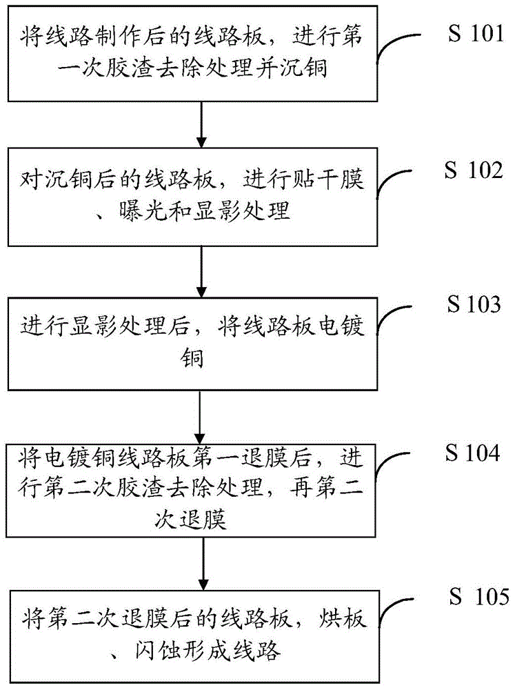
[0032] figure 1 It shows the implementation process of the fine circuit packaging substrate preparation method provided by the embodiment of the present invention, and the specific details are as follows:

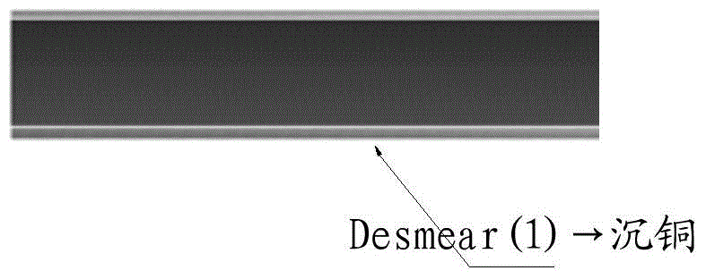
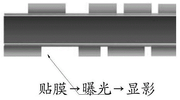
[0033] In step S101, the circuit board after the circuit is fabricated is subjected to the first smear removal treatment and copper deposition;

[0034] In the embodiment of the present invention, a copper...


PUM

PropertyMeasurementUnit
Thicknessaaaaaaaaaa

Abstract

Provided is a manufacturing method of a fine circuit packaging substrate. The method comprises the steps that primary desmear processing and copper deposition are carried out on a circuit board with a circuit manufactured; dry film sticking, exposure and developing processing are carried out on the circuit board obtained after copper deposition is carried out; after developing processing is carried out, electro-coppering is carried out on the circuit board; primary film stripping is carried out on the electro-coppered circuit board, then secondary desmear processing is carried out, and secondary film stripping is carried out; braking and flash rusting are carried out on the circuit board obtained after secondary film stripping is carried out to form a circuit. The Desmear and film stripping processes are added in the MSAP process, the fine circuit of which the L/S is 20/20 micrometers or even 18/18 micrometers, the cost caused by special copper deposition wire liquid medicine, optimal imaging film stripping liquid medicine and etching liquid medicine involved in the SAP process and special boards is avoided, and then the investment and production cost are greatly lowered.

Description

technical field [0001] The invention relates to the technical field of printed circuit boards, in particular to a fine circuit packaging substrate and a preparation method thereof. Background technique [0002] With the continuous development of the chip packaging industry and the increasingly powerful functions of intelligent equipment, the impact of its gradually smaller size has also placed higher requirements on the size and wiring density of the packaging substrate in the chip. According to the requirements of the industry for the circuit in the substrate, the ordinary design of 35 / 35um has evolved into the general 25 / 25um and the fine circuit of 18 / 18um in use. [0003] At present, the ordinary MSAP (Modified Semi-Additive Process, improved semi-additive process) process can produce circuits with a density of 25 / 25um, but there are certain difficulties in the production process for finer circuits. For ultra-fine The general process in the line industry is the SAP (Sem...

Claims


Application Information

Patent Timeline
IPC IPC(8): H05K3/46
CPCH05K3/06H05K2203/0779H05K2203/14
Inventor 崔永涛谢添华李志东
Owner GUANGZHOU FASTPRINT CIRCUIT TECH
Why Eureka
Try Eureka