Unlock instant, AI-driven research and patent intelligence for your innovation.

Memory array plane select

A technology of memory array and plane selection, applied in static memory, memory system, digital memory information, etc.

Active Publication Date: 2015-04-29
MICRON TECH INC
View PDF5 Cites 7 Cited by
  • Summary
  • Abstract
  • Description
  • Claims
  • Application Information

AI Technical Summary

Problems solved by technology

However, as the density of memory cells increases in a given area due to the decreasing size of the memory cells and / or the planes of memory cells stacked on top of each other, the footprint of the decoding logic can exceed the footprint of the memory array

Method used


Image

  • Memory array plane select
  • Memory array plane select
  • Memory array plane select

Examples


Embodiment Construction

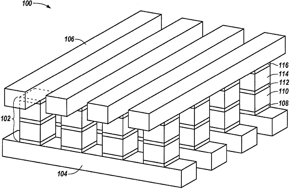
[0010] The present invention provides memory arrays and methods of forming the memory arrays. An example memory array may include at least one plane having a plurality of memory cells arranged in a matrix and a plurality of plane selection devices. Groups of the plurality of memory cells are communicatively coupled to respective ones of the plurality of plane selection devices. Decoding logic having elements formed in the substrate material and communicatively coupled to the plurality of plane selection devices. The plurality of memory cells and the plurality of plane select devices are not formed in the substrate material.

[0011] Embodiments of the invention may provide benefits such as reducing the number of elements associated with a memory array, such as transistors including decoding circuitry, formed in the substrate material. Reducing the number of elements associated with the memory array formed in the substrate material can reduce the physical footprint of the dec...


PUM


Abstract

Memory arrays and methods of forming the same are provided. An example memory array can include at least one plane having a plurality of memory cells arranged in a matrix and a plurality of plane selection devices. Groups of the plurality of memory cells are communicatively coupled to a respective one of a plurality of plane selection devices. A decode logic having elements is formed in a substrate material and communicatively coupled to the plurality of plane selection devices. The plurality of memory cells and the plurality of plane selection devices are not formed in the substrate material.

Description

technical field [0001] The present invention relates generally to semiconductor devices and methods, and more particularly to apparatus and methods for memory array plane selection. Background technique [0002] Memory devices are typically provided as internal, semiconductor, integrated circuits in computers or other electronic devices. There are many different types of memory, including random access memory (RAM), read only memory (ROM), dynamic random access memory (DRAM), synchronous dynamic random access memory (SDRAM), resistive variable memory, and flash memory, among others. memory. Types of resistance variable memory include phase change memory, programmable conductor memory, and resistive random access memory (RRAM), among others. [0003] Memory devices are utilized as non-volatile memory for a wide range of electronic applications requiring high memory density, high reliability, and data retention without power. Non-volatile memory can be used, for example, in...

Claims


Application Information

Patent Timeline
Patent Type & Authority Applications(China)
IPC IPC(8): G11C8/10
CPCG11C5/025G11C13/0004G11C2213/71G11C11/1653G11C13/0002G11C13/003G11C11/1659G11C13/0023G11C8/12G06F12/0246G11C8/10G11C11/5628G11C13/0069
Inventor 钟沅·李詹保罗·斯帕迪尼
Owner MICRON TECH INC
Features
  • R&D
  • Intellectual Property
  • Life Sciences
  • Materials
  • Tech Scout
  • Unparalleled Data Quality
  • Higher Quality Content
  • 60% Fewer Hallucinations
Learn More