Pressure-sensitive switch, manufacturing method for same, touch panel including pressure-sensitive switch, and manufacturing method for touch panel
A technology of a pressure-sensitive switch and a manufacturing method, applied in electrical switches, scattered finger contacts, contacts, etc., can solve the problems of reduced resistance value, increased contact area, deformation of resin particles, etc., achieving the effect of good accuracy and reduced deviation
- Summary
- Abstract
- Description
- Claims
- Application Information
AI Technical Summary
Problems solved by technology
Method used
Image
Examples
no. 1 Embodiment approach
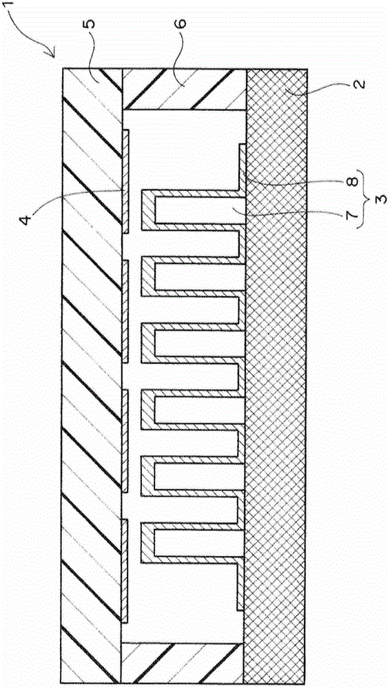
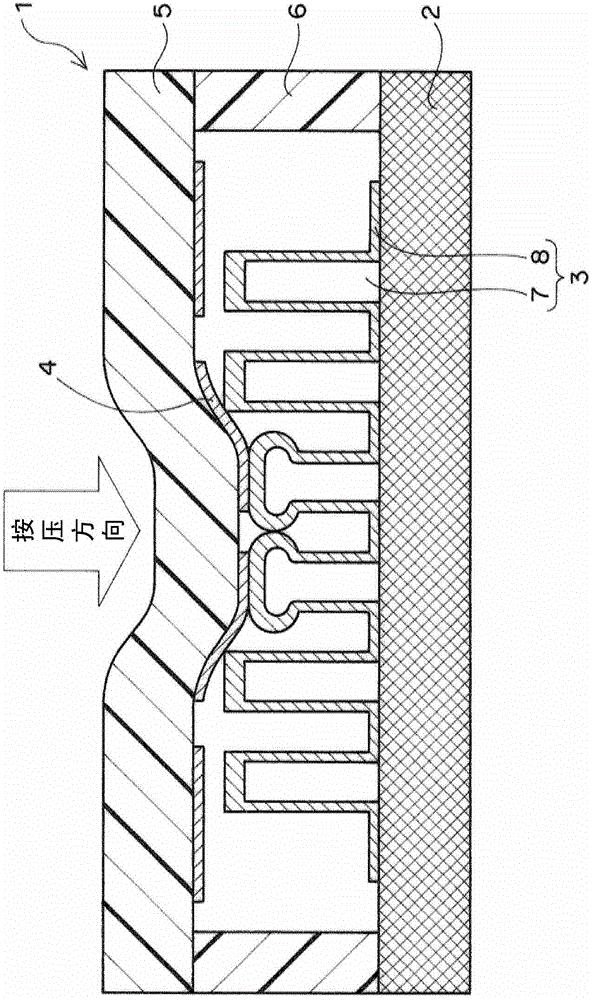
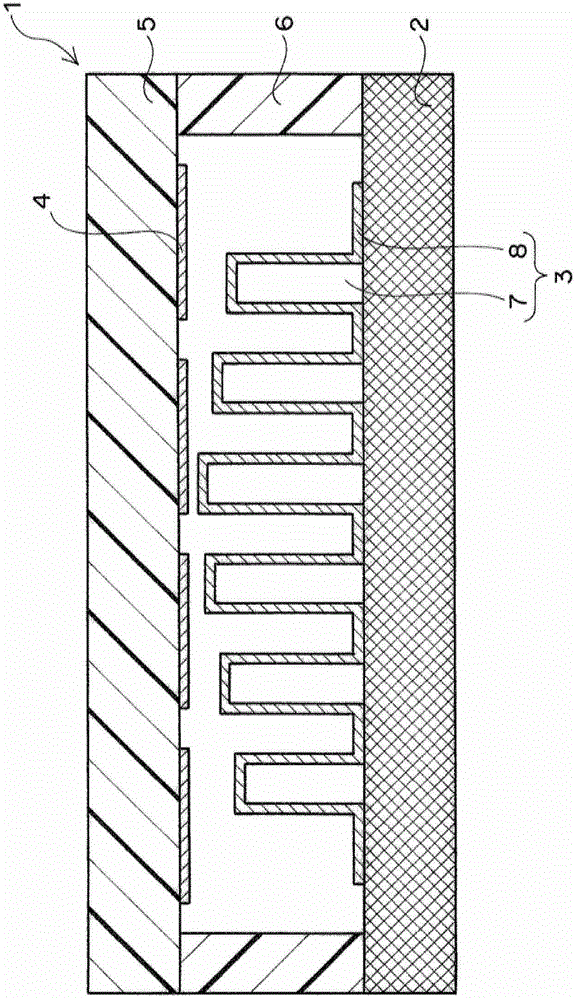
[0049] figure 1 It is a schematic cross-sectional view of the pressure sensitive switch 1 according to the first embodiment of the present invention. Such as figure 1 As shown, the pressure-sensitive switch 1 of the present invention is configured to include a support substrate 2, a conductive structure 3 provided on the support substrate 2, and a pressing base material disposed opposite to the support substrate 2 with the conductive structure 3 interposed therebetween. 5. A plurality of electrode parts 4 are provided on the pressing base material 5 . Specifically, such as figure 1 As shown, the electrode part 4 is provided on the lower surface of the pressing base material 5 . Preferably, at least two electrode parts 4 are provided on the pressing base material 5 . The pressing base material 5 is provided so as to face the support substrate 2 with the spacer 6 provided on the periphery of the support substrate 2 interposed therebetween. The separator 6 is formed of i...
no. 2 Embodiment approach
[0062] The pressure-sensitive switch of the present invention can adopt not only the above-mentioned first embodiment but also the following second embodiment. A pressure-sensitive switch according to a second embodiment of the present invention will be described below.
[0063] The pressure-sensitive switch 1 of the present invention is configured to include a support substrate 2 , a conductive structure 3 provided on the support substrate 2 , and a pressing base 5 provided above the conductive structure 3 . The conductive structure 3 includes an elastic structural member 9 provided to continuously protrude from the support substrate 2 , and an electrode layer 10 formed to cover the elastic structural member 9 . The so-called elastic structural member 9 protruding continuously from the support substrate 2 refers to: Figure 8 (3) The form in which the elastic structural member 9 is arranged on the support substrate 2 in a grid pattern as shown, or Figure 8 (4) A form in wh...
PUM
 Abstract
Description
Claims
Application Information


