Liquid crystal display device, driving control circuit and driving method used in same

a technology of liquid crystal display device and control circuit, which is applied in the direction of electric digital data processing, instruments, computing, etc., can solve the problems of increasing scale and power consumption, affecting the viewing experience of users, and the conventional liquid crystal display device described above has the following problems, so as to reduce the occurrence of a variation in luminance in an upper and lower portion of the display screen, and reduce the blurring of moving images

Active Publication Date: 2007-10-04
NEC LCD TECH CORP
View PDF2 Cites 48 Cited by
  • Summary
  • Abstract
  • Description
  • Claims
  • Application Information

AI Technical Summary

Benefits of technology

[0028]With the above configuration, the field dividing driving operation is performed in which an odd field and an even field occur repeatedly and the odd / even field is divided into the first odd / even sub-field and second odd / even sub-field and, during the period of the first odd / even sub-field, display data corresponding to an input video signal is line-sequentially written in each of pixel regions and, during the period of the second odd / even sub-field, dark data is line-sequentially written to each of the pixel regions and, therefore, an operational frequency of a signal for each component can be reduced to half. As a result, if a frequency for switching between the odd field and even field is the same as a frame frequency, the conventional doubled increase in frequency caused by black insertion driving can be offset by a by-half decrease in frequency achieved by the driving method of the present invention, which enables the provision of the liquid crystal display device capable of reducing blurring of moving images without causing doubling in operational frequency of a signal for each component, and a driving control circuit and driving method employed in the liquid crystal display device. Further, by setting the frequency for switching between the odd and even fields at a frequency being twice higher than the frame frequency, a doubled increase in frequency caused by the increased frame frequency can be offset by the by-half decrease in frequency achieved by the driving method of the present invention and, therefore, at the operational frequency of the signal for each component being the same as the conventional frequency for black insertion driving, a flashing frequency for black display and video display can be doubled, which enables the provision of the liquid crystal display device capable of reducing blurring of moving images and flickering caused by black insertion, and the driving control circuit and driving method employed in the liquid crystal display device. In addition, since time required for holding display data and black data in each of pixel regions corresponding to each scanning electrode is made equal, the occurrence of a variation in luminance in an upper portion and lower portion of the display screen can be prevented.
[0029]With another configuration as above, the polarity of a voltage of data to be written in each of the pixel regions corresponding to the scanning electrodes in odd-numbered rows is inverted in every odd field and the polarity of a voltage of data to be written in each of the pixel regions corresponding to the scanning electrodes in even-numbered rows is inverted in every even field and, therefore, biasing of the polarity of a voltage of display data depending on regions of the liquid crystal display panel is reduced and screen burn-in can be decreased. As a result, if the frequency for switching between the odd field and even field is the same as the frame frequency, time for holding black data as dark data is made longer and, therefore, even in the liquid crystal display panel in which the effect of black insertion cannot be exploited fully due to a slow response time from all white to all black such as an IPS (In-Plane Switching)-type liquid crystal, black insertion driving can be easily achieved. Furthermore, in the odd field, each of the scanning electrodes in the odd-numbered rows is successively driven and, at the same time, each of the scanning electrodes in the even-numbered rows existing next to the scanning electrodes in the odd-numbered rows is successively driven, which improves luminance efficiency of the liquid crystal display device.

Problems solved by technology

However, in conventional liquid crystal displays, when moving images are displayed, while a current image remains persistent in a user's consciousness, a subsequent image is displayed, which causes an afterimage (trail-leaving and / or blurring of moving images) to be seen by users.
However, the conventional liquid crystal display device described above has following problems.
That is, the liquid crystal display device shown in FIG. 18 presents a problem in that, an operational frequency for each component doubles when compared with the case of no black insertion driving and, therefore, hardware configurations corresponding to the doubled driving frequency are required, as a result, causing an increase in scale and in power consumption.
Also, the conventional liquid crystal display device presents another problem in that each of the scanning electrodes is line-sequentially driven and, as shown in FIG. 20, the polarity of a voltage of display data D is inverted on every line and this inverted pattern is reversed again per every refresh rate and, therefore, the polarity of the voltage of display data is biased in some regions on the liquid crystal display panel, causing the occurrence of a screen burn-in.
In addition, though the problem of trail-leaving is improved by black insertion driving, alternate flashing occurs between the time for black display and time for video display in a frequency band in which a human can recognize, which causes an increase of flickering on a screen.
In order to suppress the flickering, a refresh rate needs to be raised to a degree to which a human cannot recognize, which, as a result, the operational frequency doubled by the black insertion driving is further increased twice, thus causing a difficulty in hardware configurations.
Hei 04-044478 presents a problem in that, though an operational frequency of a signal for each component is allowed to be made lower by performing the interlaced driving operation, since, in the latter half of an odd field, black data is simultaneously written in each of pixel regions corresponding to all the odd-numbered rows of scanning electrodes and, in the latter half of the even field, black data is simultaneously written in each of the pixel regions corresponding to all the even-numbered rows of scanning electrodes, time for holding the written black data varies on every line, which causes a variation in luminance between an upper part and lower part of a display screen.

Method used


Image

  • Liquid crystal display device, driving control circuit and driving method used in same
  • Liquid crystal display device, driving control circuit and driving method used in same
  • Liquid crystal display device, driving control circuit and driving method used in same

Examples


first embodiment

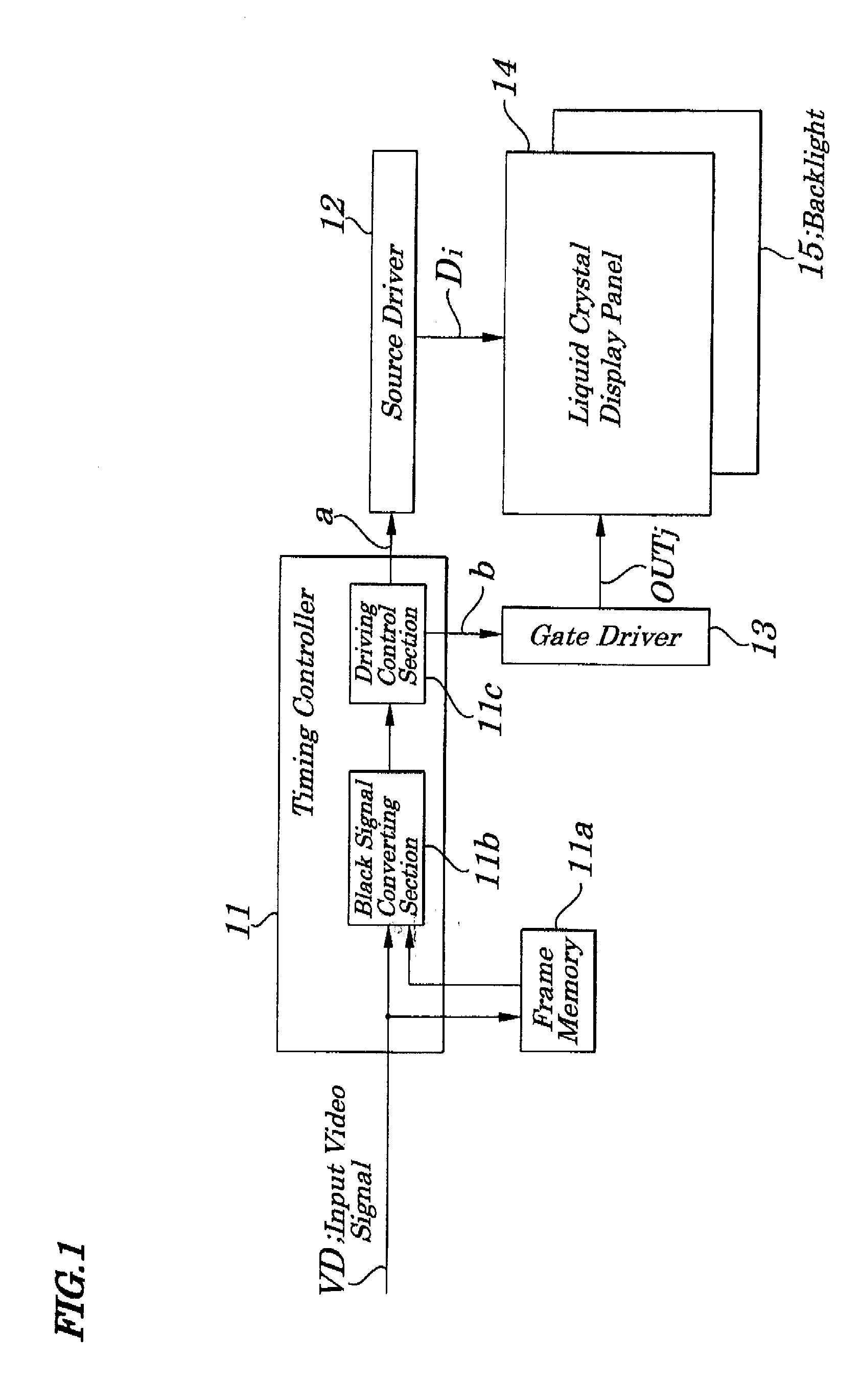
[0053]FIG. 1 is a block diagram showing electrical configurations of main components of a liquid crystal display device of the first embodiment of the present invention. The liquid crystal display device of the first embodiment, as shown in FIG. 1, includes a timing controller 11, a source driver 12, a gate driver 13, a liquid crystal display panel 14, and a backlight 15.

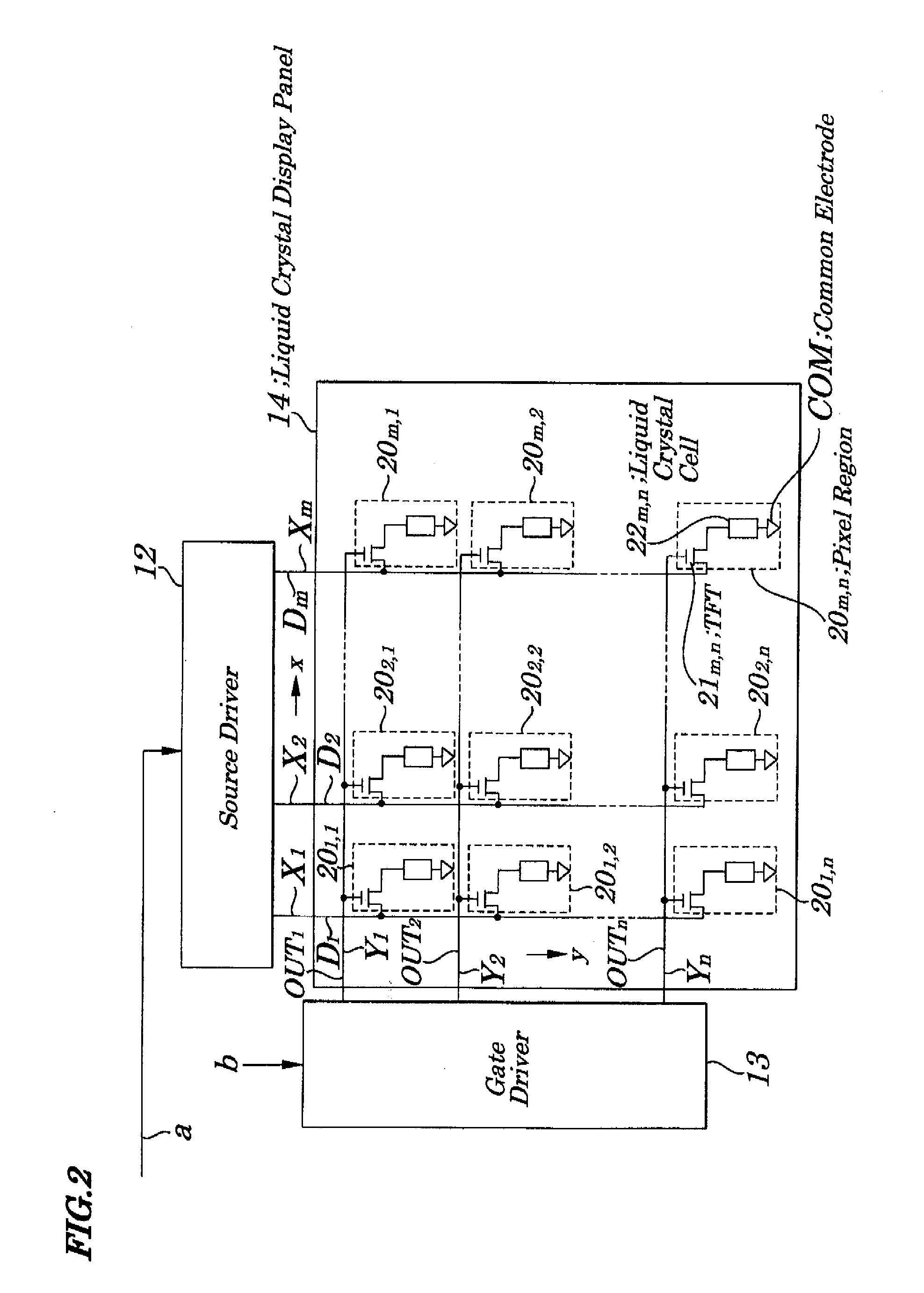
[0054]FIG. 2 is a schematic diagram showing one example of electrical configurations of the liquid crystal display panel of FIG. 1. The liquid crystal display panel 14 is of a transmissive-type that permits light from the backlight to come in and in which, as shown in FIG. 2, a plurality of columns of data electrodes Xi (i=1, 2, . . . , m, for example, m=640×3), a plurality of rows of scanning electrodes Yj (j=1, 2, . . . , n; for example, n=480) so arranged as to be orthogonal to the data electrodes Xi, and pixel regions 20i,j. Each of the data electrodes Xi is formed at specified intervals in an x direction and re...

second embodiment

[0068]FIG. 11 is a time chart explaining operations of a liquid crystal display device according to a second embodiment of the present invention. FIG. 12 is a diagram explaining the inversion of the polarity of a voltage of data to be written in each of pixel regions of the second embodiment. FIG. 13 is a waveform diagram explaining operations of the liquid crystal display device of the second embodiment. FIG. 14 is a diagram showing another example of the inversion of the polarity of a voltage of data to be written in each of the pixel regions according to the second embodiment. FIG. 15 is a diagram showing still another example of the inversion of the polarity of a voltage of data to be written in each of the pixel regions according to the second embodiment. FIG. 16 is a diagram showing yet another example of the inversion of the polarity of a voltage of data to be written in each of the pixel regions of the second embodiment. Processing of the driving method employed in the liqui...

third embodiment

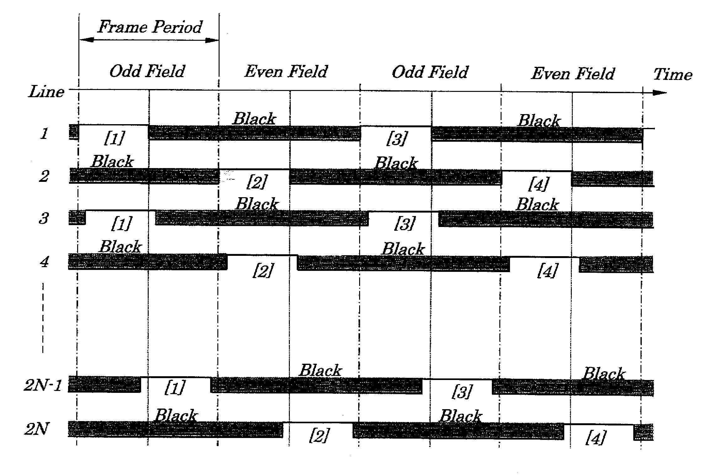
[0071]FIG. 17 is a time chart explaining a modified example of operations of the liquid crystal display according to a third embodiment of the present invention. The liquid crystal display device of the first embodiment is driven at a frequency being a half the frequency at which black is inserted ordinarily. In the third embodiment, in the case where the liquid crystal display panel and each component are driven at a doubled speed, one frame is divided into four fields and, by setting the frequency for switching between the odd and even field at a frequency being twice higher than a frame frequency, a doubled increase in frequency caused by an increased frame frequency can be offset by the by-half decrease in frequency achieved by the driving method of the present invention. Therefore, at an operational frequency of a signal of each component being the same as the conventional frequency for black insertion driving, a flashing frequency for black display and video display can be dou...


PUM


Abstract

A liquid crystal display device is provided which is capable of improving quality of moving images. A field dividing driving operation is performed in which an odd field during which each of scanning electrodes in odd-numbered rows is sequentially driven and an even field during which each of scanning electrodes in even-numbered rows is sequentially driven occur, alternately and repeatedly, with time width of a refresh rate. In the former half of the odd field, display data is written in each of pixel regions corresponding to scanning electrodes in odd-numbered rows and, in the latter half of the odd field, black data is written in each of the pixel regions corresponding to scanning electrodes in the odd-numbered rows. In the former half of the even field, display data is written in each of pixel regions corresponding to scanning electrodes in the even-numbered rows and, in the latter half of the even field, black data is written in each of pixel regions corresponding to scanning electrodes in the even-numbered rows.

Description

BACKGROUND OF THE INVENTION[0001]1. Field of the Invention[0002]The present invention relates to a liquid crystal display device and to a driving control circuit and driving method to be used in the liquid crystal display, and more particularly to the liquid crystal display device suitably used for displaying moving images and to the driving control circuit and driving method to be used in the liquid crystal display device.[0003]The present application claims priorities of Japanese Patent Application Nos. 2006-101252 filed on Mar. 31, 2006 and 2006-159001 filed on Jun. 7, 2006, which are hereby incorporated by reference.[0004]2. Description of the Related Art[0005]In recent years, a liquid crystal display device is used not only as a monitor of personal computers but also as a display for television sets or a like. In its application to television sets, performance of displaying moving images is required. However, in conventional liquid crystal displays, when moving images are displ...

Claims


Application Information

Patent Timeline
Patent Type & Authority Applications(United States)
IPC IPC(8): G09G3/36
CPCG09G3/3614G09G3/3648G09G2310/0224G09G2320/0261G09G2320/0233G09G2320/0257G09G2310/061
Inventor KIMURA, HIROAKI
Owner NEC LCD TECH CORP
Why Eureka
Try Eureka