Chip measuring sorting system and method

A sorting system and chip technology, which is applied in semiconductor/solid-state device testing/measurement, electrical components, semiconductor/solid-state device manufacturing, etc., can solve the problems of high production cost and low production efficiency, so as to improve work efficiency and reduce hardware Cost and labor cost, effect of reducing process steps

Active Publication Date: 2015-05-06
EPITOP PHOTOELECTRIC TECH
View PDF6 Cites 11 Cited by
  • Summary
  • Abstract
  • Description
  • Claims
  • Application Information

AI Technical Summary

Problems solved by technology

[0005] The present invention provides a chip measurement and sorting system and method to solve the problem of low production efficiency and low production effi

Method used


Image

  • Chip measuring sorting system and method
  • Chip measuring sorting system and method
  • Chip measuring sorting system and method

Examples


Example Embodiment

[0028] In order to make the objectives, technical solutions, and advantages of the embodiments of the present invention clearer, the technical solutions in the embodiments of the present invention will be described clearly and completely in conjunction with the accompanying drawings in the embodiments of the present invention. Obviously, the described embodiments It is a part of the embodiments of the present invention, not all the embodiments. Based on the embodiments of the present invention, all other embodiments obtained by those of ordinary skill in the art without creative work shall fall within the protection scope of the present invention.

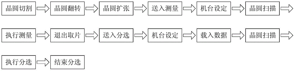
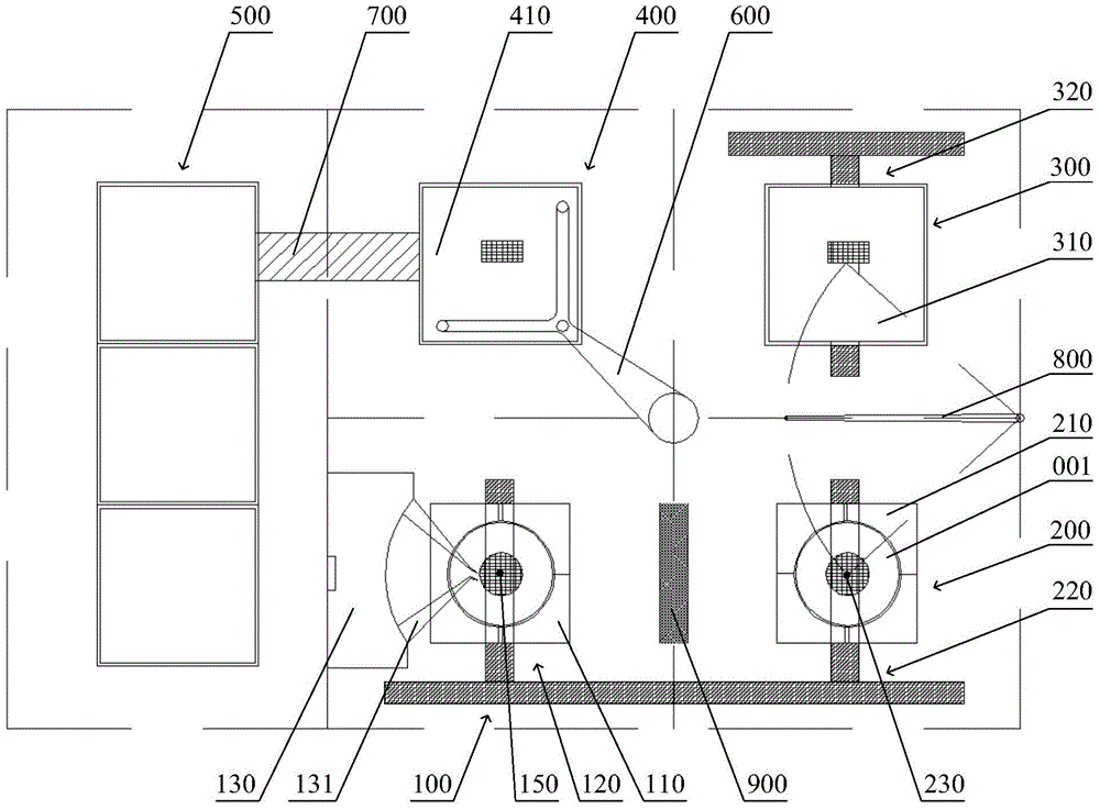
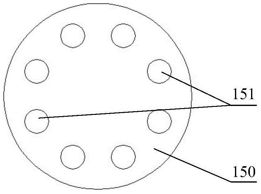
[0029] In the following specific embodiments of the present invention, the specific structure of the measurement and sorting system of the chip proposed by the present invention and the connection relationship and working mode of the various devices of the system in the working state are explained through a more detailed implementation...


PUM


Abstract

The invention provides chip measuring sorting system and method. The system comprises a sorting device, a measuring device and a carrying device, wherein the sorting device and the measuring device are adjacent to each other; a first storing seat is arranged in the measuring device, and while a second sorting seat is arranged in the sorting device; the carrying device is adjacent to a positioning access device; a first carrying platform is arranged on the carrying device, and while a second carrying platform is arranged on the positioning access device to carry and position a standard device; the carrying device is adjacent to the storing device; a picking rotating arm is arranged between the carrying device and the sorting device; the positioning access device is arranged adjacent to a tool frame assembly, and a second mechanical arm is arranged between the positioning access device and the device frame assembly; a standard device and a central control system which is connected with all the devices above are stored in the device frame assembly. With the adoption of the system, the problems of low production efficiency and relatively high production cost due to repeated setting of a cabinet and wafer scanning during measuring and sorting chips in the prior art can be solved.

Description

technical field [0001] The invention relates to semiconductor manufacturing technology, in particular to a chip measurement and sorting system and method. Background technique [0002] After the semiconductor wafer is thinned and diced on the back side, thousands of independent chips are formed, which usually need to be sorted according to the characteristics of each chip in the wafer. For example, the sorting of LED chips is usually based on the LED The photoelectric characteristics of the chip, that is, it is necessary to classify thousands of chips in the wafer according to different photoelectric characteristics, and discard the damaged or abnormal chips. This process is called sorting. [0003] At present, before sorting LED chips, all LED chips in the wafer are measured one by one to obtain the photoelectric characteristics of each chip; specifically, the measurement and sorting of the wafer usually includes the following steps: The photoelectric characteristics of ea...

Claims


Application Information

Patent Timeline
IPC IPC(8): H01L21/67
CPCH01L21/67242H01L21/67271H01L22/14
Inventor 姚禹郑远志陈向东康建梁旭东
Owner EPITOP PHOTOELECTRIC TECH
Why Eureka
Try Eureka