a led light bulb

A technology of LED light bulbs and LED chips, applied in the field of LED lighting, can solve the problems of interference between LED light-emitting substrates, difficulty in increasing heat dissipation, scattered light, etc., and achieve the effects of improving light extraction efficiency, eliminating light spot interference, and improving heat dissipation effect

Inactive Publication Date: 2018-09-07
陈宗烈
View PDF15 Cites 0 Cited by
  • Summary
  • Abstract
  • Description
  • Claims
  • Application Information

AI Technical Summary

Problems solved by technology

The light is scattered and not concentrated: it is difficult for the light emitted from different points in a plane to be concentrated with a uniform and orderly reflective structure. Therefore, a secondary light output design (configuration of the light output angle) must be carried out, but the secondary light distribution will inevitably reduce the light output. Efficiency; the contradiction between brightness and volume: If in order to increase the brightness, it is necessary to increase the light-emitting area (that is, increase R) and make the made lighting fixtures bulky, but with the increase of the area, the difficulty of secondary light distribution increases and the cost increases , the problem of light scattered and not concentrated is more prominent; it is difficult to dissipate heat: since it is directly mounted on a plane, even if a substrate material with good heat dissipation is used and a heat sink is used to dissipate heat, due to the existence of the LED light-emitting substrate substrate, a large The thermal resistance of the substrate causes the temperature of the substrate to rise, the power density of the chip mounting is high, the heat peak of the chip is high, and the heat dissipation is difficult to increase; the light spot interference is mainly the interference between the scattered LED light-emitting substrates.

Method used


Image

  • a led light bulb
  • a led light bulb
  • a led light bulb

Examples


Embodiment Construction

[0026] First, let's explain the two terms and their meanings used in the following description of the present application.

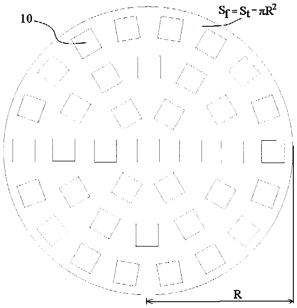
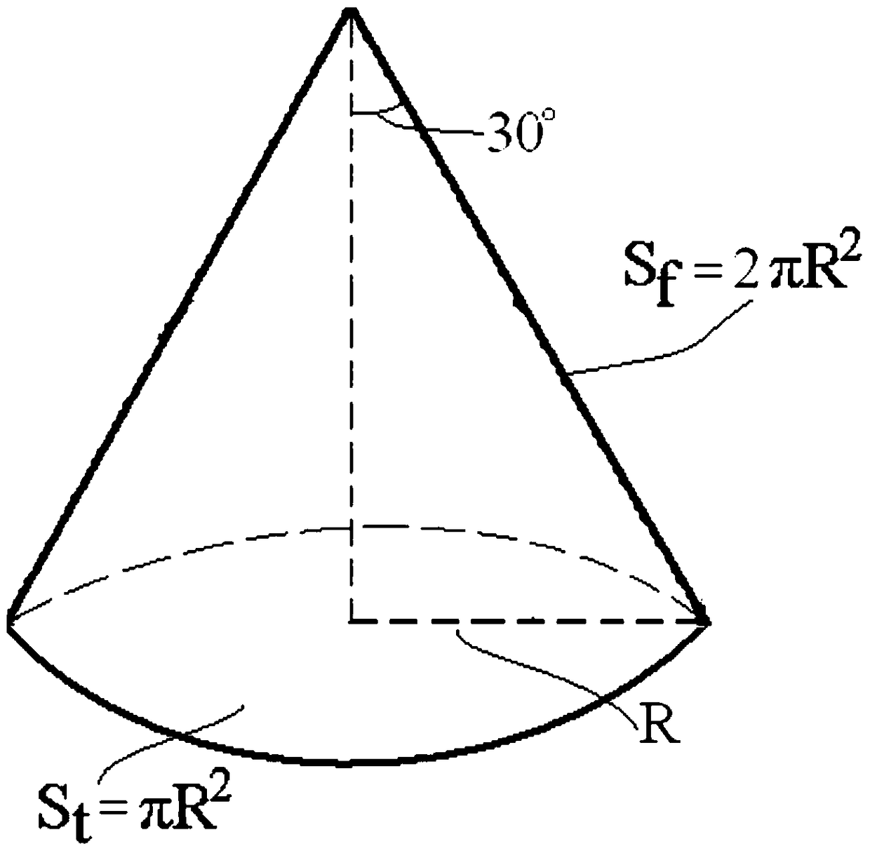
[0027] Light emitting area S f : Refers to the area of ​​the surface from which light is emitted. For example in figure 1 The circular surface of the light-emitting LED chips is covered in an array, and its light-emitting area is πR 2 ;

[0028] Light area S t : The area of ​​the optical channel bounded by the physical boundaries. Also refer to figure 1 The circular surface of the light-emitting LED chips is covered in an array. If the circular surface is considered to be a straight cylinder bottom, the light emitted from the bottom of the cylinder will pass through the cylinder opening along the cylinder wall. The area of ​​the cylinder opening is the light transmission area S t .

[0029] According to the above description, it can be understood that the figure 1 In the case of the circular surface covered with light-emitting LED chips in an arr...


PUM


Abstract

The invention relates to an LED lamp bulb. The LED lamp bulb comprises a lamp holder, a transparent lamp cup and an LED chip array, and the outer surface of the transparent lamp cup is provided with a light reflection structure and a reflection layer which are used for reflecting light; the LED chip array is directly pasted to the inner surface of the transparent lamp cup; in addition, LED chips in the LED chip array comprise vestigial substrates which range from 0.1 micrometer to 1 micrometer.

Description

technical field [0001] The invention relates to the field of LED lighting, in particular to an LED lighting fixture made of LED chips, that is, an LED light bulb. Background technique [0002] LED lighting is already widely used in industry, for example as a backlight for liquid crystal displays. Moreover, in terms of the application of energy-saving and green daily lighting that can be seen in the future, the development of LED lighting fixtures is undoubtedly the first choice. [0003] However, the currently developed LED lighting products still have various problems and cannot replace the current ordinary energy-saving lamps, such as insufficient brightness, poor heat dissipation, light components that are not suitable for human eye lighting, spot interference, and non-concentrated light areas, etc. . [0004] figure 1 The light-emitting surface of a prior art LED lighting lamp is shown. Among them, an LED array formed by a plurality of light-emitting LED chips is mou...

Claims


Application Information

Patent Timeline
Patent Type & Authority Patents(China)
IPC IPC(8): F21K9/23F21V3/04F21V19/00F21V29/503F21Y115/10
CPCF21V3/061F21V19/001
Inventor 陈宗烈
Owner 陈宗烈
Why Eureka
Try Eureka