
Eureka
For R&D, Eureka makes reading and utilizing patents & technical documents easy.
Eureka AIR
Designed for self-driven R&D workflows. Generate viable solutions, solve complex R&D challenges, empower your innovation with AI.

Eureka Materials
Designed for material experts only. Revolutionize your material R&D, from search, analyze, to developing new materials.

TechResearch
Generate reliable direction feasibility study reports for your R&D in just a few steps.

TechSeek
Discover and master advanced knowledge NOW. Basics, ideas, possibilities, all at once.

TechMind
As an expert in R&D Theories, TechMind can generates customized viable solutions instantly.

TechRisk
Analyze your overall solution with one click, know your potential R&D risks in advance.

TechMonitor
Get weekly tech updates, stay abreast of the latest tech innovations and key insights.
Method of manufacturing semiconductor chip, semiconductor chip, and semiconductor device
A manufacturing method and semiconductor technology, applied in semiconductor/solid-state device manufacturing, semiconductor devices, semiconductor/solid-state device components, etc., can solve problems such as low impact resistance, low chip flexural strength, and longer cutting time, and achieve high productivity effect
- Summary
- Abstract
- Description
- Claims
- Application Information
AI Technical Summary
Problems solved by technology
Method used
Image

Examples
Embodiment Construction
[0060] Hereinafter, embodiments of the present invention will be described with reference to the drawings.
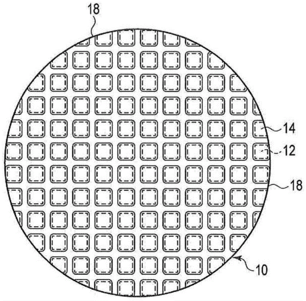
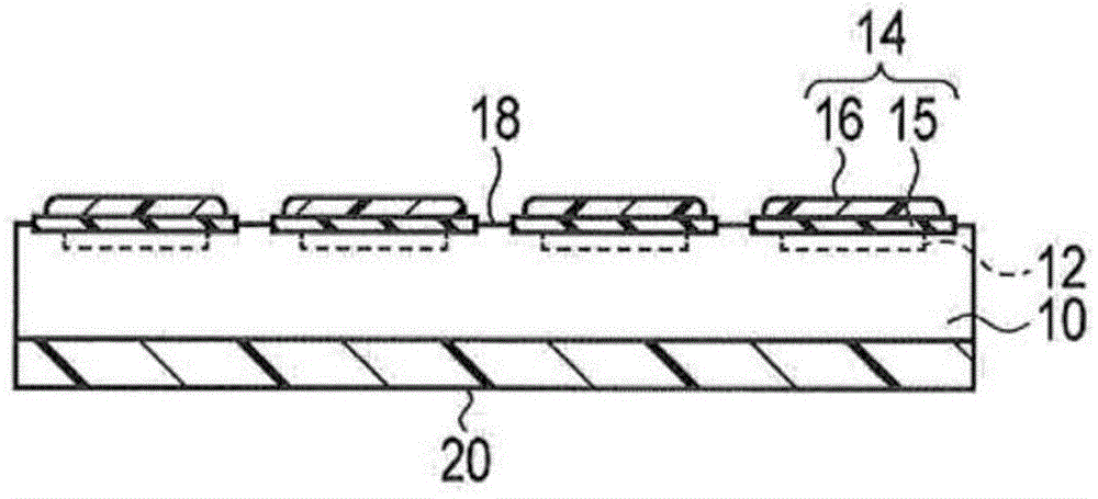
[0061] figure 1 It is a top view of a semiconductor substrate used in the method of one embodiment. figure 2 express figure 1 A partial cross-sectional view of a semiconductor device.
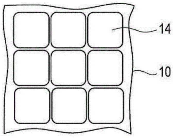
[0062] As shown in the figure, a plurality of element regions 12 are provided on a semiconductor substrate 10, and each element region 12 includes one or more semiconductor elements. These element regions 12 are arranged separately from each other. Each element region 12 is covered and protected by an etching mask 14 .
[0063] The semiconductor elements included in the element region 12 are, for example, transistors, diodes, light emitting diodes, or semiconductor lasers. The element region 12 may further include capacitors, wiring, and the like.
[0064]A region between adjacent element regions 12 is an exposed region 18 where the surface of the semiconductor substrate 10 is exp...
PUM
 Abstract
Description
Claims
Application Information
 - R&D Engineer
- R&D Manager
- IP Professional
- Industry Leading Data Capabilities
- Powerful AI technology
- Patent DNA Extraction
Browse by: Latest US Patents, China's latest patents, Technical Efficacy Thesaurus, Application Domain, Technology Topic, Popular Technical Reports.
© 2024 PatSnap. All rights reserved.Legal|Privacy policy|Modern Slavery Act Transparency Statement|Sitemap|About US| Contact US: help@patsnap.com