Array substrate, preparation method thereof, and display device

An array substrate and substrate technology, which is applied in the field of flat panel display, can solve problems such as disconnection of pixel electrodes and affect the display effect of the display device, and achieve the effects of preventing disconnection of pixel electrodes, improving display effect, and simple operation

Active Publication Date: 2015-05-27
SHANGHAI TIANMA MICRO ELECTRONICS CO LTD +1
View PDF9 Cites 13 Cited by
  • Summary
  • Abstract
  • Description
  • Claims
  • Application Information

AI Technical Summary

Problems solved by technology

[0003] In recent years, thin display devices have become more and more sought after by consumers. There are many ways to prepare thin display devices, among which the method of making touch electrodes in liquid crystal cells is particularly common. Usually, touch electrodes are made in On the TFT substrate of the display device, it is necessary to make a shielding electrode on the TFT substrate, and when the shielding electrode is etched, the coated shielding electrode in the contact hole electrically connected to the pixel electrode and the drain of the thin film transistor Over-etching, during the etching process, the drain metal in the contact hole will be over-etched, forming an inverted cone (Taper) structure, resulting in disconnection of the pixel electrode on the upper drain, thus affecting the display effect of the display device

Method used


Image

  • Array substrate, preparation method thereof, and display device
  • Array substrate, preparation method thereof, and display device
  • Array substrate, preparation method thereof, and display device

Examples


Embodiment Construction

[0021] The technical solutions in the embodiments of the present invention will be clearly and completely described below in conjunction with the accompanying drawings in the embodiments of the present invention. Obviously, the described embodiments are only a part of the embodiments of the present invention, rather than all the embodiments. Based on the embodiments of the present invention, all other embodiments obtained by those of ordinary skill in the art without creative work shall fall within the protection scope of the present invention.

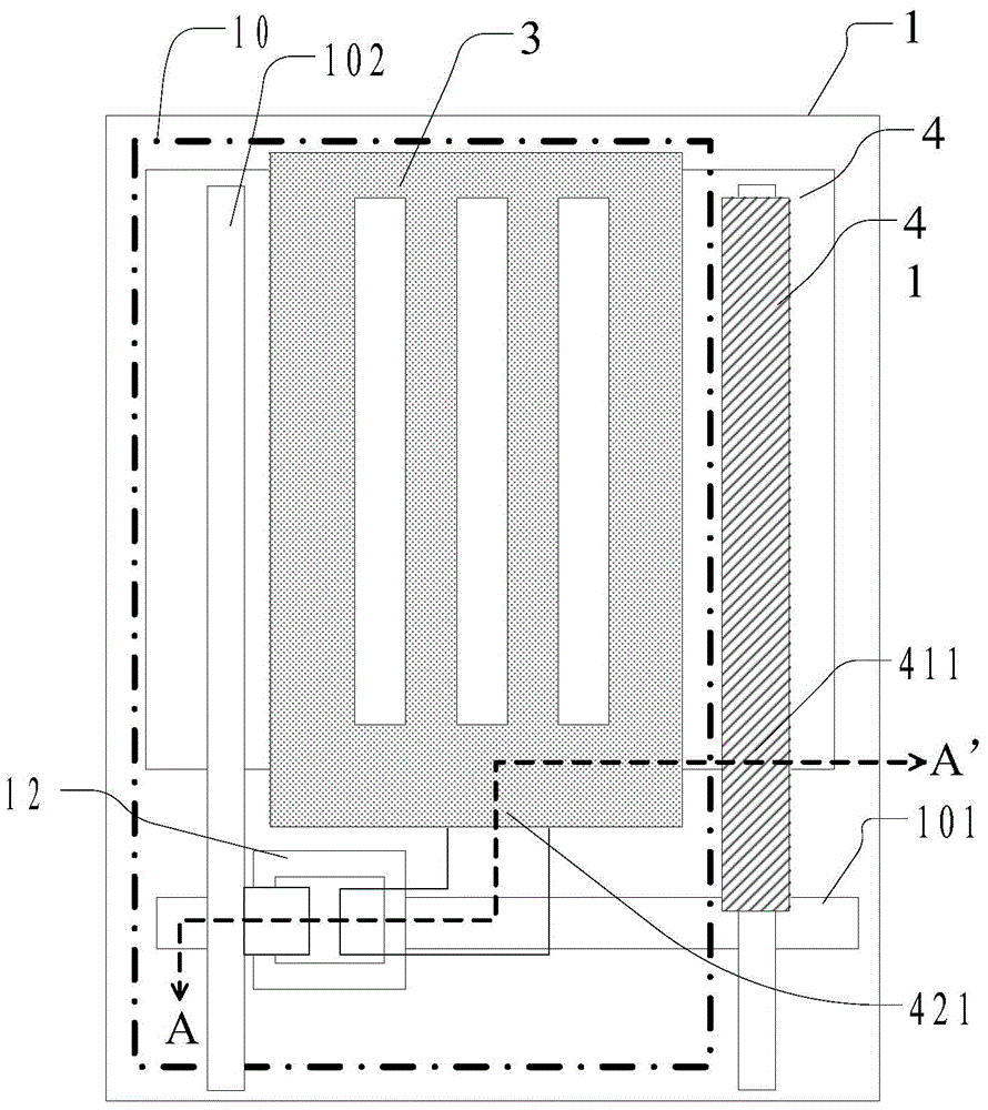
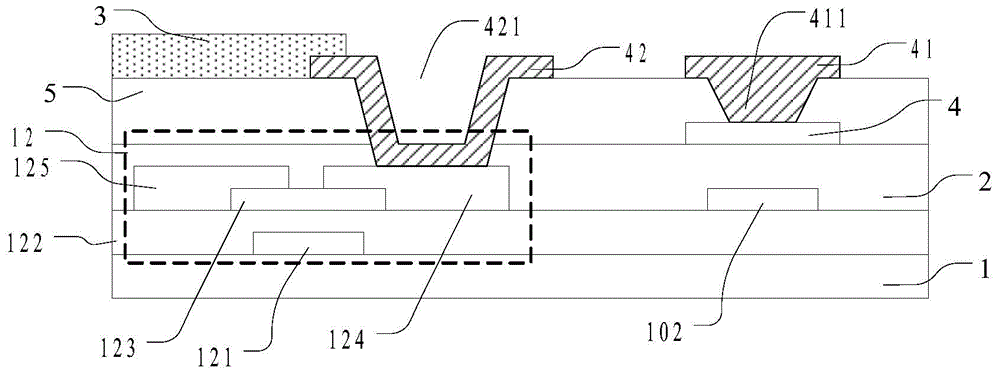
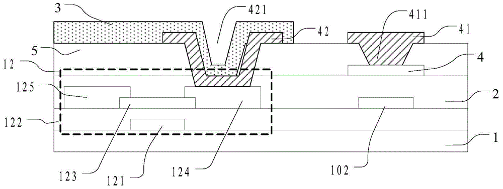
[0022] The embodiment of the present invention provides an array substrate, such as figure 1 with figure 2 As shown, the array substrate includes a substrate 1; a plurality of gate lines 101, a plurality of data lines 102, and a plurality of first signal lines 41 are provided on the substrate, and the gate lines 101 and the data The lines 102 are insulated and cross each other to define a plurality of pixel units 10; the pixel units incl...


PUM


Abstract

The invention discloses an array substrate, a preparation method thereof, and a display device comprising the array substrate. A first through hole through which part of a first electrode is exposed is arranged in a pixel switch; a first protective layer is arranged in the first through hole; a pixel electrode is electrically connected with the first electrode through the first protective layer; the protective layer and a first signal line are of the same metal layer; the first signal line provides an electric signal to a common electrode. Through the structural design, the drain metal in the first through hole can be effectively prevented from over-etching, so that the pixel electrode on the upper layer of a drain is prevented from being broken; therefore, the display effect of the display device is improved; moreover, the preparation method of forming the first signal line and the first protective layer on a third insulating layer in which the first through hole and a second through hole are formed is adopted, wherein the first protective layer is formed in the first through hole; in addition, the preparation method is easy to operate.

Description

Technical field [0001] The present invention relates to flat panel display technology, in particular to an array substrate and a preparation method thereof, and a display device including the array substrate. Background technique [0002] Display panels are currently widely used in mobile phones, handheld computers (Personal Digital Assistant, PDA) and other portable electronic products, such as: Thin Film Transistor-Liquid Crystal Display (TFT-LCD), organic light-emitting diodes Displays (Organic Light Emitting Diode, OLED), Low Temperature Poly-silicon (LTPS) displays, and Plasma Display Panels (PDP), etc. Driven by market competition, display devices that are lighter, have better display effects, and have lower prices are increasingly sought after. [0003] In recent years, thin display devices have been increasingly sought after by consumers. There are currently many methods to prepare thin display devices. Among them, the method of fabricating touch electrodes in liquid cryst...

Claims


Application Information

Patent Timeline
Patent Type & Authority Applications(China)
IPC IPC(8): G02F1/1362G02F1/1368H01L23/50
CPCG02F1/136227G02F1/1368G02F1/136295H01L27/1244H01L27/1259
Inventor 武丽娟王征董倩
Owner SHANGHAI TIANMA MICRO ELECTRONICS CO LTD
Why Eureka
Try Eureka