
Active Matrix Electroluminescence Display Device

An electroluminescent display, active matrix technology, applied in circuits, electrical components, electrical solid devices, etc., can solve the threshold voltage shift of thin film transistors, the data multiplexer drive circuit cannot operate normally, and thin film transistors cannot be completely turned off, etc. problem, to achieve the effect of reducing electrical offset

Active Publication Date: 2018-04-10
INNOLUX CORP
View PDF3 Cites 0 Cited by
  • Summary
  • Abstract
  • Description
  • Claims
  • Application Information

AI Technical Summary

Problems solved by technology

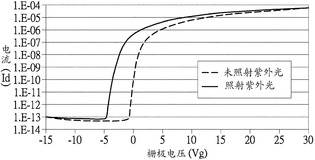
like Figure 1B As shown, after the traditional active matrix electroluminescent display device is irradiated by ultraviolet light, it causes a significant shift in the threshold voltage (Vth) of the thin film transistor
[0003] Therefore, due to the ultraviolet light or external ultraviolet light in the organic light-emitting diode process, the thin-film transistor will cause the thin-film transistor to not be completely turned off (light leakage in the dark state) and shift when the organic light-emitting diode display is operated in a dark state. Register (Shift Register, S / R), data multiplexer (Data Mux) and other drive circuits cannot operate normally, etc.

Method used


Image

  • Active Matrix Electroluminescence Display Device
  • Active Matrix Electroluminescence Display Device
  • Active Matrix Electroluminescence Display Device

Examples


no. 1 example

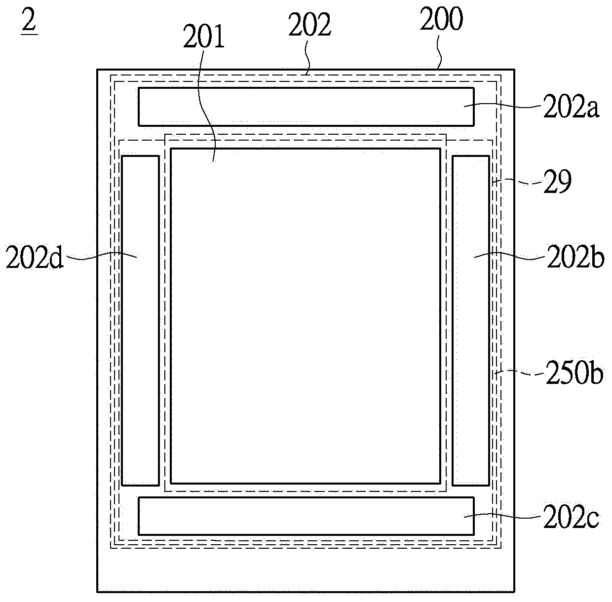
[0037] Please also refer to Figure 2A and Figure 3A , Figure 2A is a plan view of the active matrix electroluminescence display device provided by the first embodiment of the present invention, Figure 3A It is a cross-sectional view of the active matrix electroluminescent display device provided by the embodiment of the present invention. The active matrix electroluminescent display device 2 includes a substrate 200, a plurality of first transistor elements 220, a first electrode layer 250a, an organic light emitting layer 250b, a second electrode layer 250c and a plurality of second transistor elements 220'. The substrate 200 may be glass. The substrate 200 includes a top surface 200 a on which a light emitting region 201 and a peripheral circuit region 202 located on the periphery of the light emitting region 201 are formed. The top surface 200a of the substrate 200 faces an incident direction of ambient light. Such as Figure 2A The peripheral circuit region 202 s...


PUM


Abstract

An active matrix electroluminescence display device, which includes a substrate, a plurality of first transistor elements, a first electrode layer, an organic light-emitting layer, a second electrode layer and a plurality of second transistor elements. The top surface of the substrate has a light emitting area and a peripheral circuit area located around the light emitting area. The plurality of first transistor elements and the plurality of second transistor elements are respectively located in the light-emitting area and the peripheral circuit area of ​​the substrate. The first electrode layer, the organic light-emitting layer and the second electrode layer are stacked on the substrate in sequence, and cooperate to form a plurality of organic light-emitting diodes arranged in an array in the light-emitting area to form a plurality of pixels, and these first transistor elements are respectively The organic light emitting diodes are electrically connected to control the organic light emitting diodes to emit light, and the organic light emitting layer covers at least one second transistor element.

Description

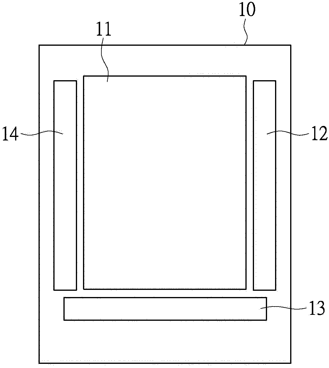
technical field [0001] The present invention relates to a display device, and in particular to an active matrix electroluminescence display device. Background technique [0002] Organic light emitting diodes have been used in displays. Such as Figure 1A As shown, a light emitting region 11 and three peripheral circuit regions 12 , 13 , 14 are disposed on the substrate 10 , and the peripheral circuit regions 12 , 13 , 14 are adjacent to the light emitting region 11 . However, since the active layer material of the thin film transistor (TFT) in the peripheral circuit area (12, 13 or 14) in the display has an energy gap close to that of ultraviolet (UV) light, the TFT element is quite sensitive to ultraviolet light . Irradiating ultraviolet light is a commonly used procedure in the display process, and after irradiating ultraviolet light, additional electron-hole pairs will be generated, which will cause extra electrons on the channel of the thin film transistor, causing the...

Claims


Application Information

Patent Timeline
Patent Type & Authority Patents(China)
IPC IPC(8): H01L27/32H01L23/552
Inventor 黄浩榕沈义和杨朝森
Owner INNOLUX CORP
Learn More