Method for manufacturing metallization groove holes in PCB

A technology of metallization groove and manufacturing method, which is applied in the direction of printed circuit manufacturing, electrical connection formation of printed components, electrical components, etc., can solve problems such as irregular shape of slot holes, and achieve the effect of improving quality

Active Publication Date: 2015-06-17
大连崇达电子有限公司
View PDF11 Cites 11 Cited by
  • Summary
  • Abstract
  • Description
  • Claims
  • Application Information

AI Technical Summary

Problems solved by technology

[0003] The present invention aims at the problem that the shape of the produced slots is irregular due to the asymmetry of the positions of the drilled holes when making the metallized slots in the PCB in the prior art, and provides a method for making high-precision metallized slots. Methods

Method used


Image

  • Method for manufacturing metallization groove holes in PCB
  • Method for manufacturing metallization groove holes in PCB
  • Method for manufacturing metallization groove holes in PCB

Examples


Embodiment

[0017] This embodiment provides a method for manufacturing metallized slots in a PCB, and the specific manufacturing steps are as follows:

[0018] (1) Pressing to form a multi-layer board

[0019] Firstly, as in the production process of the PCB in the prior art, the raw materials of the PCB are cut to obtain a core board, and then the inner layer circuit is produced on the core board by using a negative film process. Through the AOI inspection of the inner layer, check whether there are defects such as open and short circuits, line gaps, and line pinholes in the inner layer lines, and products without defects enter the lamination process.

[0020] The first choice is to brown the core board, then stack the core board, prepreg and outer copper foil according to the design data, and then select the appropriate pressing conditions according to the Tg of the board to press the stacked boards into one. Form a multi-layer board.

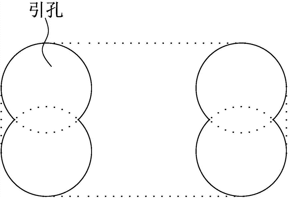
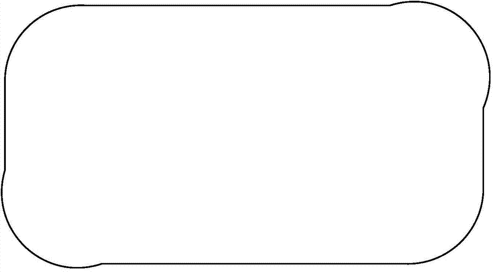
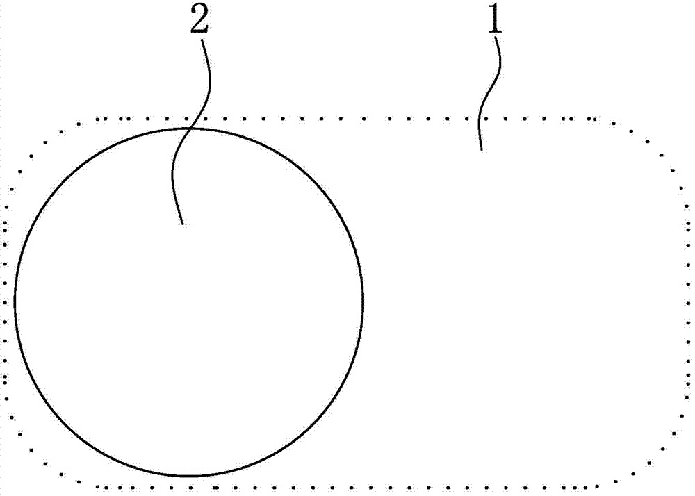
[0021] (2) Milling slot hole

[0022] Drill a g...


PUM


Abstract

The invention relates to the technical field of manufacturing of PCBs, in particular to a method for manufacturing metallization groove holes in a PCB. The method comprises the steps that a guiding hole is drilled in each hole position where a metallization groove hole needs to be manufactured in a multilayer board, and then a milling cutter is used for conducting milling along the shape of the hole positions from the guiding holes to manufacture the groove holes. Due to the fact that only one guiding hole is formed in each hole position, the problem of asymmetry of the guiding holes does not exist, so that the problem that the manufactured groove holes are special-shaped holes due to the asymmetry of the positions of the drilled guiding holes is solved, it is ensured that the shape and the appearance of the metallization groove holes meet the design requirements, and the quality of the PCB is improved.

Description

technical field [0001] The invention relates to the technical field of PCB manufacture, in particular to a method for manufacturing metallized slots in a PCB. Background technique [0002] PCB (Printed Circuit Board), the Chinese name is printed circuit board, referred to as printed board, is one of the important components of the electronics industry, is the support of electronic components, and the carrier of electrical connections. With the continuous improvement of functionality, precision and quality requirements of electronic equipment, the quality requirements of PCB are also getting higher and higher. In PCB production, in order to meet some special design requirements, it is necessary to make metallized slots on the PCB, and the chamfers in the fabricated metallized slots are required to be uniform. In the existing PCB production, usually when making the slot hole, the lead holes are first drilled around the position of the slot hole to be made, such as figure 1 A...

Claims


Application Information

Patent Timeline
Patent Type & Authority Applications(China)
IPC IPC(8): H05K3/42
CPCH05K3/0047H05K3/425H05K2201/09563H05K2201/09854H05K2203/0214
Inventor 翟青霞林楠李金龙刘东白会斌
Owner 大连崇达电子有限公司
Why Eureka
Try Eureka