TEM sample support film and its preparation method, TEM sample analysis method

A technology that supports membranes and samples, applied in the semiconductor field, can solve problems affecting analysis results and achieve the effect of less time

Active Publication Date: 2017-12-29
SEMICON MFG INT (SHANGHAI) CORP
View PDF9 Cites 0 Cited by
  • Summary
  • Abstract
  • Description
  • Claims
  • Application Information

AI Technical Summary

Problems solved by technology

[0010] In view of the above-mentioned shortcoming of the prior art, the object of the present invention is to provide a kind of TEM sample carrying net support film and its preparation method, and TEM analysis method, be used to solve the carbon film in the prior art as image problem in TEM analysis Problems that affect the results of the analysis

Method used


Image

  • TEM sample support film and its preparation method, TEM sample analysis method
  • TEM sample support film and its preparation method, TEM sample analysis method
  • TEM sample support film and its preparation method, TEM sample analysis method

Examples


Embodiment Construction

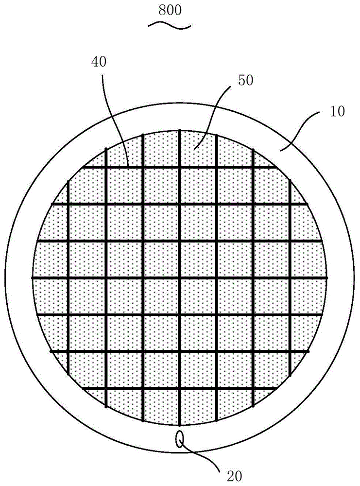
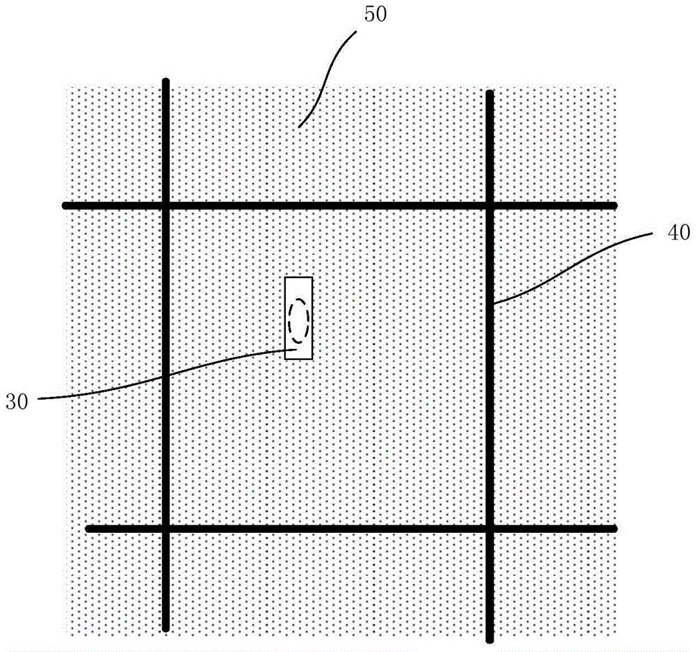
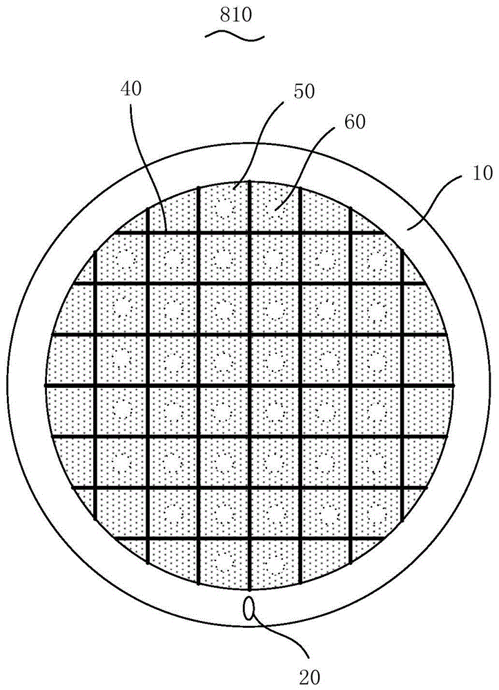
[0054]The inventor of the present invention has improved the TEM sample carrying network support film in the traditional technology through many tests and summaries, and provided a new TEM sample carrying network support film, including: a carrying component, and the carrying component is set There is a hollowed out area, and the hollowed out area includes a plurality of hollowed out parts; a carbon film is covered on the hollowed out area; wherein, at least one of the carbon films covered on the hollowed out part is provided with a sample hole.

[0055] When the new TEM sample grid support membrane is used for TEM analysis, the TEM sample is placed on the sample hole, and the target area to be analyzed in the TEM sample is aligned with the sample hole, so that the TEM analysis is carried out At this time, the carbon film will not become the background of the TEM sample, affecting the observation and analysis of the TEM analysis. The carbon film on the edge of the sample hole ...


PUM


Abstract

The invention provides a TEM sample carrying network supporting film, a preparation method thereof, and a TEM sample analysis method. Wherein, the TEM sample carrier grid support film at least includes: a carrying component, a hollowed out area is provided in the carrying component, and a plurality of hollowed out parts are included in the hollowed out area; a carbon film is covered on the hollowed out area; wherein, A sample hole is arranged in the carbon film covered on at least one of the hollow parts. The sample holes provided on the carbon film of the TEM sample grid support film are suitable for avoiding the TEM sample from being affected by the carbon film when performing TEM analysis, and can be firmly adsorbed on the carbon film at the same time, and obtain sufficient carbon film. support.

Description

technical field [0001] The invention relates to the technical field of semiconductors, in particular to a TEM sample carrying grid support film, a preparation method thereof, and a TEM sample analysis method. Background technique [0002] At present, TEM (Transmission electron microscope, lens electron microscope) is increasingly used to observe the morphology of semiconductor devices and conduct failure analysis on semiconductor devices. The main working principle of TEM is to project the accelerated and concentrated electron beam onto a very thin sample, and the electrons collide with the atoms in the sample to change the direction, thereby producing solid angle scattering. The size of the scattering angle is related to the density and thickness of the sample, so images with different brightness and darkness can be formed, and then the images can be observed, measured and analyzed later. In performing TEM analysis, the sample determines the accuracy of the TEM analysis st...

Claims


Application Information

Patent Timeline
Patent Type & Authority Patents(China)
IPC IPC(8): G01Q30/20G01Q30/00
Inventor 于会生段淑卿陈柳赵燕丽郭志蓉
Owner SEMICON MFG INT (SHANGHAI) CORP
Why Eureka
Try Eureka