LED device packaged in system-level mode

A technology for LED devices and system-level packaging, applied in the direction of electric solid devices, semiconductor devices, electrical components, etc., can solve the problems of low degree of integration, many process procedures, and high cost, to simplify product structure, simplify packaging process, cost reduced effect

Active Publication Date: 2015-06-24
SICHUAN SUNFOR LIGHT
View PDF4 Cites 1 Cited by
  • Summary
  • Abstract
  • Description
  • Claims
  • Application Information

AI Technical Summary

Problems solved by technology

Moreover, the application has a relatively low degree of integration, and its novelty and innovation are not high
Moreover, its structure is complex, the process procedures are more, and the cost is higher

Method used


Image

  • LED device packaged in system-level mode
  • LED device packaged in system-level mode
  • LED device packaged in system-level mode

Examples


Embodiment Construction

[0031] The present invention will be described in detail below in conjunction with the accompanying drawings.

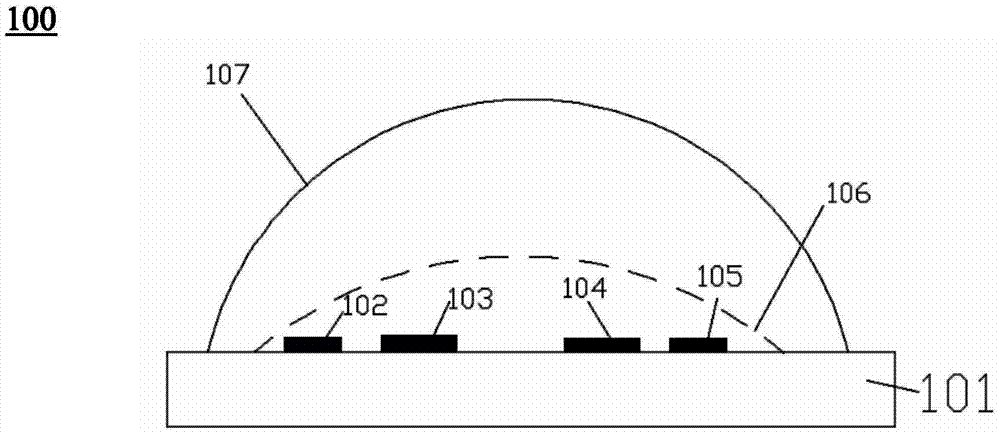
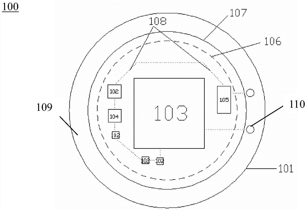
[0032] figure 1 and figure 2 Both show a system-in-package LED device 100 , which includes a substrate 101 , a driving circuit element 102 and an LED chip 103 . The system-in-package LED device 100 also includes at least one functional module. The driving circuit element 102, the LED chip 103 and the functional modules are all fixed on the only substrate 101 by means of die bonding. Moreover, the driving circuit element 102 , the LED chip 103 and the functional modules are all electrically connected to the substrate 101 by gold wire welding, so as to realize a highly integrated system-in-package of the LED device 100 on the only substrate 101 . Compared with traditional LED packaging devices, the system-in-package LED device 100 of the present invention adds functional modules on the basis of original components, such as figure 1104 and 105 shown in , make LED l...


PUM


Abstract

The invention relates to an LED device packaged in a system-level mode. The LED device comprises a substrate, a drive circuit element and an LED chip and is characterized by further comprising a control chip module and a wireless communication module. The drive circuit element, the LED chip, the control chip module and the wireless communication module are fixed to the substrate together in a solid crystallization mode. The drive circuit element, the LED chip, the control chip module and the wireless communication module are electrically connected with the substrate in a gold wire welding mode, so that the LED device is highly integrated on the only substrate and packaged in the system-level mode. The LED device packaged in the system-level mode meets the requirements for high integration, the small size and the multiple functions.

Description

technical field [0001] The invention relates to an LED device, in particular to a system-in-package LED device. Background technique [0002] LED products are widely used in the lighting and display industry due to their advantages of energy saving, power saving, high efficiency, fast response time, long life cycle, mercury-free, and environmental benefits, and have become one of the most eye-catching products in recent years. . Traditional LED lamps are composed of light sources, driving circuits, thermal devices and optical devices, and each part is independent. Wherein the driving circuit is processed and packaged with the bare chip of the electronic component, and then welded on the printed circuit board with solder. The packaged electronic component has a large volume size, which makes the volume of the driving circuit board larger. Therefore, in the structural design of traditional lamps, a cavity is specially reserved to place the drive circuit, such as a bulb lamp;...

Claims


Application Information

Patent Timeline
Patent Type & Authority Applications(China)
IPC IPC(8): H01L33/48H01L33/58H01L33/60
CPCH01L25/0753H01L33/48H01L33/58H01L33/60
Inventor 罗超林莉贾晋李东明
Owner SICHUAN SUNFOR LIGHT
Why Eureka
Try Eureka