Flexible display and manufacturing method thereof

A flexible display and manufacturing method technology, applied in semiconductor/solid-state device manufacturing, static indicators, instruments, etc., can solve the problems of fragile brackets, reduced display deformability, and unfavorable high-end intelligence

Active Publication Date: 2015-07-01
CHENGDU VISTAR OPTEOLECTRONICS CO LTD
View PDF5 Cites 17 Cited by
  • Summary
  • Abstract
  • Description
  • Claims
  • Application Information

AI Technical Summary

Problems solved by technology

However, with long-term use, the hinge is easy to fail, and the bracket is also easy to damage, and the addition of rigid materials will reduce the deformability of the display,

Method used


Image

  • Flexible display and manufacturing method thereof
  • Flexible display and manufacturing method thereof
  • Flexible display and manufacturing method thereof

Examples


Embodiment 1

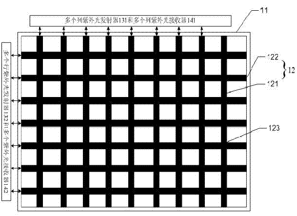
[0027] Such as figure 1 and figure 2 Shown is a schematic structural diagram of a flexible display. The flexible display in this embodiment is an active matrix organic light-emitting display (AMOLED), 11 is a flexible substrate, and a display device (not shown) and a first array are arranged on the flexible substrate 11. circuit (not shown). Preferably, the flexible substrate is an organic polymer PI, and of course, metal or glass can also be selected as the flexible substrate material as required. The display device includes active matrix organic light emitting diodes, pixel electrodes, common electrodes, and the like. The first array circuit is composed of data lines and gate lines distributed in a matrix, two adjacent data lines and gate lines enclose a rectangular area, and each rectangular area corresponds to a pixel. The flexible display also includes a front plate (not shown) positioned on top of the flexible display.

[0028] The second array circuit 12 is arrange...

Embodiment 2

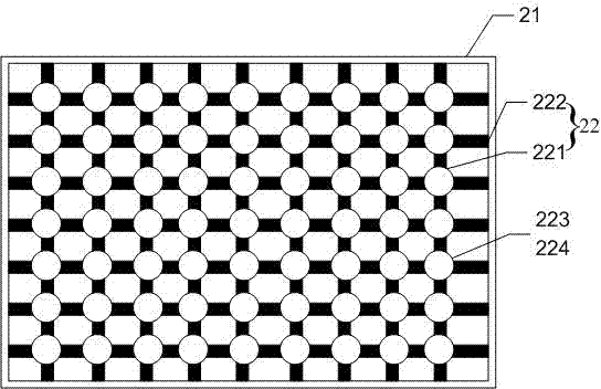
[0044] Such as Figure 4 and Figure 5 As shown, it is a schematic structural diagram of a flexible display. The flexible display in this embodiment is an active matrix organic light-emitting display (AMOLED), 21 is a flexible substrate, and a display device (not shown) and a first array circuit are arranged on the flexible substrate. (not shown). The flexible substrate is organic polymer PI, and of course metal or glass can also be selected as the flexible substrate material according to needs. The display device includes active matrix organic light emitting diodes, pixel electrodes, common electrodes, and the like. The first array circuit is composed of data lines and gate lines distributed in a matrix, two adjacent data lines and gate lines enclose a rectangular area, and each rectangular area corresponds to a pixel. The flexible display also includes a front plate (not shown) positioned on top of the flexible display.

[0045] A second array circuit 22 is arranged on t...


PUM


Abstract

The invention discloses a flexible display, so as to realize folding or extending of the flexible display and realize real-time 3D animation display according to user needs. The flexible display comprises a flexible substrate, a display device arranged on the flexible substrate, and an array circuit. Lines of the array circuit are distributed above or below the flexible substrate in an array mode and are crossed to form multiple crossing points. The array circuit is wholly or partially made of a shape memory material. The shape memory material generates deformation under physical excitation and can be recovered. The invention also provides a flexible display manufacturing method. The method comprises steps: the flexible substrate is manufactured and the display device is manufactured on the flexible substrate; the shape memory material is wholly or partially deposited above or below the flexible substrate; photoetching technology is used for manufacturing the array circuit whose lines are distributed in an array mode and crossed to form multiple crossing points; and the shape memory material generates deformation under physical excitation and can be recovered.

Description

technical field [0001] The invention relates to a flexible display and a manufacturing method thereof, in particular to a flexible display using a shape memory material and a manufacturing method thereof. Background technique [0002] A flexible display refers to a display device with a bendable display panel, which includes flexible organic electroluminescent displays (OLEDs), flexible electrophoretic displays (EPDs), flexible liquid crystal displays (LCDs) and other types. As a new generation of display devices, because of its thin and light, high contrast, fast response, wide viewing angle, high brightness, full color and other advantages, it is widely used in mobile phones, personal digital assistants (PDA), digital cameras, car displays, notebook computers, etc. , wall-mounted TV, and military fields have very broad application prospects. [0003] What is used in flexible displays is a flexible substrate, which is made of a flexible material that can be bent, allowing ...

Claims


Application Information

Patent Timeline
IPC IPC(8): G09G3/32H01L27/32H01L51/56G02F1/1333G02F1/167G09G3/3225
Inventor 习王锋施露蔡世星
Owner CHENGDU VISTAR OPTEOLECTRONICS CO LTD
Why Eureka
Try Eureka