

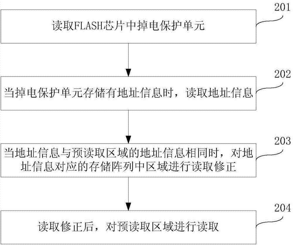
Read method for responding to FLASH chip abnormal power-down
A chip and abnormal technology, applied in the field of memory, can solve the problems of reducing the reliability of FLASH chips, reducing the accuracy of data recorded by FLASH chips, and misreading of FLASH chips, so as to reduce misreading, improve reliability, and improve accuracy.
- Summary
- Abstract
- Description
- Claims
- Application Information
AI Technical Summary
Problems solved by technology
Method used
Image

Examples
Embodiment Construction
[0025] The present invention will be described in more detail and complete below in conjunction with the accompanying drawings and specific embodiments. It should be understood that the specific embodiments described here are only used to explain the present invention, but not to limit the present invention. In addition, it should be noted that, for the convenience of description, only parts related to the present invention are shown in the drawings but not all content.
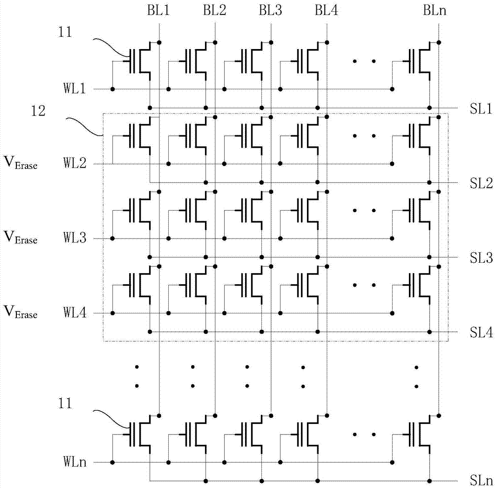
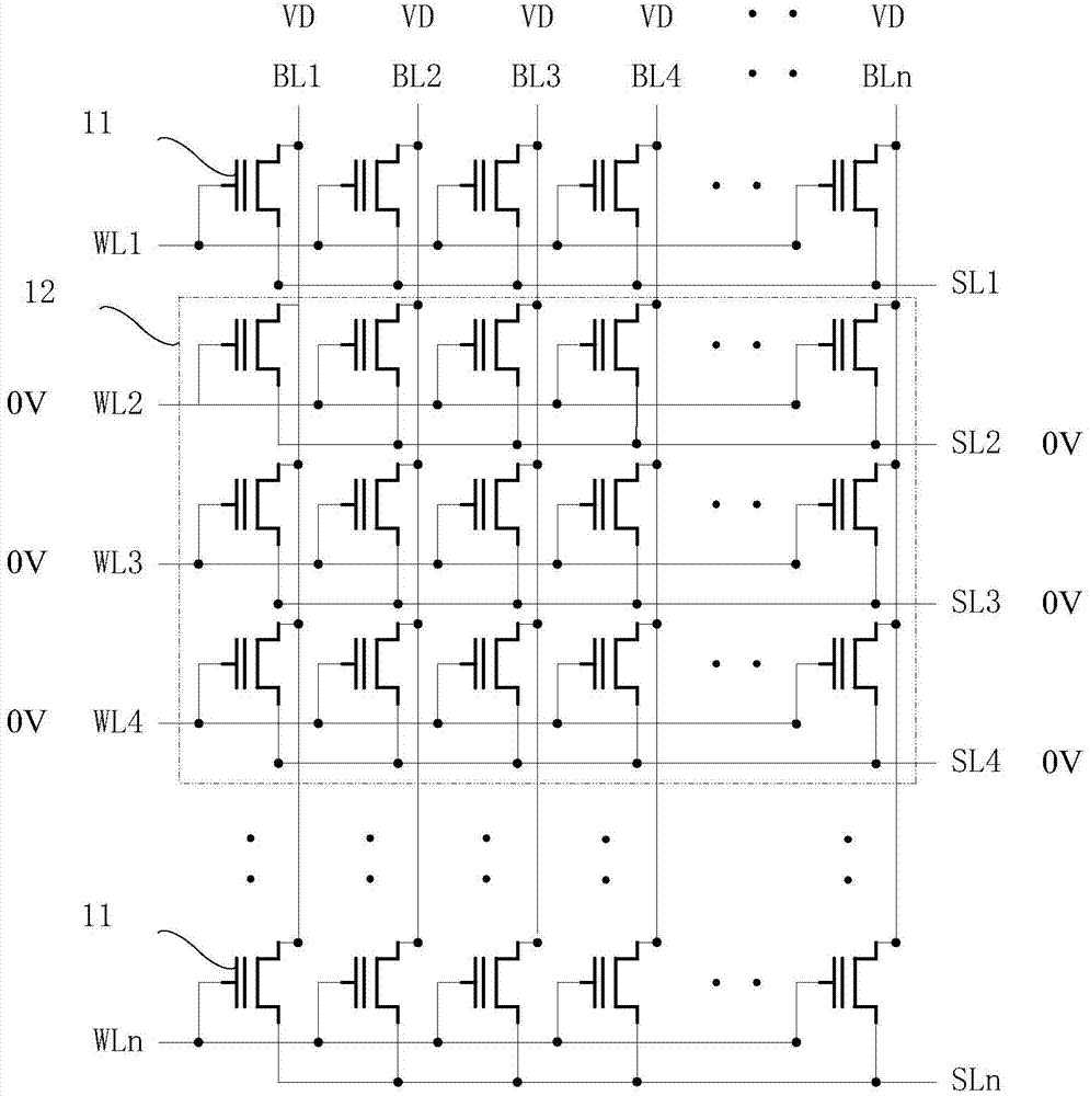
[0026] FLASH is composed of storage units (cells). Usually, a memory cell includes source (source, S), drain (drain, D), control gate (controlling gate, CG), and floating gate (floating gate, FG), and the control gate can be used for Connect to the reference voltage VG. If the drain is connected to the reference voltage VD, the voltage VG is applied to the control gate CG and the source S is connected to the ground, the memory cell realizes the channel hot electron injection programming operation. For eras...
PUM
 Abstract
Description
Claims
Application Information