
Copper plating solution capable of realizing co-plating of through hole, blind hole and circuit

A blind hole and circuit technology, applied in the field of copper plating solution, can solve the problem of not seeing

Inactive Publication Date: 2015-07-08
AKM ELECTRONICS TECH SUZHOU
View PDF9 Cites 20 Cited by
  • Summary
  • Abstract
  • Description
  • Claims
  • Application Information

AI Technical Summary

Problems solved by technology

Therefore, it leads to the development of a full copper filling that can satisfy blind holes and fill through holes (usually 100% full copper filling is not required, but the copper thickness of the hole usually needs to reach 15um or more), and it must also be able to meet the pattern electroplating production line requirements, there is no such medicine on the market

Method used


Image

  • Copper plating solution capable of realizing co-plating of through hole, blind hole and circuit

Examples


Embodiment 1

[0016] The ratio of copper plating solution is as follows:

[0017] Copper Methanesulfonate 200g / L

[0018] Methanesulfonic acid 30g / L

[0019] Hydrochloric acid 50mg / L

[0020] Accelerator 0.7mL / L

[0021] Inhibitor 10mL / L

[0022] Leveling agent 15mL / L

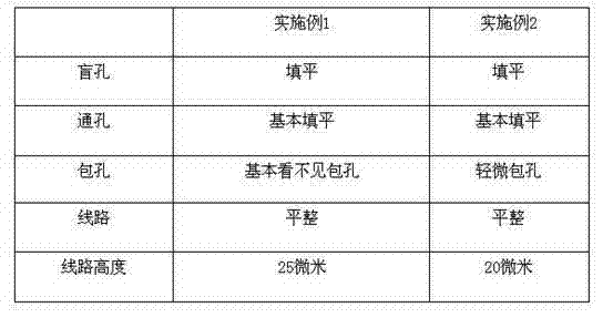
[0023] The methanesulfonic acid system copper plating solution prepared by the above scheme adopts 0.5ASD and the electroplating time is 4h. The results obtained are shown in Table 1: the blind hole is filled and the through hole is basically filled and leveled. , the line height is 25μm, without bottom copper.

Embodiment 2

[0025] The copper plating solution of methanesulfonic acid system prepared by the above scheme also adopts 0.7ASD, and the electroplating time is 3h. Flat, the line height is 20μm, without bottom copper.

[0026]


PUM


Abstract

The invention provides a copper plating solution capable of realizing co-plating of a through hole, a blind hole and a circuit, which belongs to the field of manufacturing of circuit boards. The copper plating solution is characterized by comprising the following components: copper methanesulfonate, methanesulfonic acid, hydrochloric acid, an accelerator, an inhibitor and a leveling agent. The copper plating solution has the following advantages: the copper plating solution can realize full copper filling of the blind hole and filling of the through hole and meet requirements of pattern plating in practical production; on the premise that smoothness of the circuit is good, the blind hole can be effectively filled up and mad even, the through hole is basically filled up and mad even, hole wrapping conditions are substantially improved, and the qualified ratio of products is substantially increased; and the copper plating solution effectively overcomes the problem that different copper plating solutions are needed for production of package substrates and further improves the wiring density of substrate products.

Description

technical field [0001] The invention relates to a copper plating solution for co-plating through holes, blind holes and lines. Background technique [0002] Electroplating is a key process in printed circuit boards and semiconductor packaging substrates. At present, electroplating is mainly used for electrical interconnection between layers of printed circuit boards. With the development of application technology, the increase of wiring density and the increase of high-power devices , the heat dissipation requirements of the packaging substrate are becoming more and more significant. For high-density packaging substrates, the structure contains a large number of through holes and blind holes. Blind holes or through holes are generally located in the center of the pad. In order to effectively increase the density of wiring, the aperture of blind holes or through holes must be small enough. Usually 30~100μm. Of course, there may also be some heat conduction holes. The heat c...

Claims


Application Information

Patent Timeline
IPC IPC(8): C25D3/38
CPCC25D3/38
Inventor 王靖
Owner AKM ELECTRONICS TECH SUZHOU
Learn More