
Liquid crystal display panel, manufacturing method for liquid crystal display panel and liquid crystal display device

A liquid crystal display panel and liquid crystal droplet technology, which is applied in the directions of instruments, nonlinear optics, optics, etc., can solve the problems of liquid crystal droplets being difficult to flow, surrounding light leakage, pollution, etc., and achieve the effect of reducing surrounding pollution.

Active Publication Date: 2015-07-08
HEFEI BOE OPTOELECTRONIC TECH CO LTD +1
View PDF5 Cites 3 Cited by
  • Summary
  • Abstract
  • Description
  • Claims
  • Application Information

AI Technical Summary

Problems solved by technology

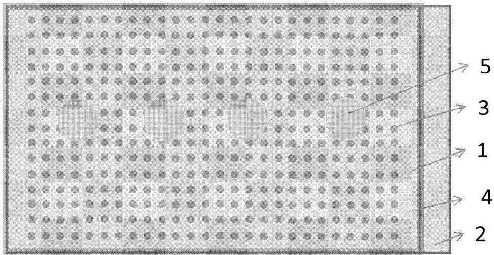
However, in this liquid crystal pattern layout, the liquid crystal drops are likely to be in contact with the sealant, especially in the direction where the liquid crystal drops have a short flow distance, causing contamination, such as peripheral friction marks (Mura), punctures, and peripheral light leakage ( Zara), not filled, and bubbles (Bubble) and other undesirable phenomena, resulting in the existence of peripheral friction marks (Mura) and other adverse phenomena in existing small-sized TFT-LCD devices
In addition, in the existing small-size TFT-LCD devices, due to the existing liquid crystal layout pattern design, the liquid crystal droplets are not easy to flow to the corners of the device

Method used


Image

  • Liquid crystal display panel, manufacturing method for liquid crystal display panel and liquid crystal display device
  • Liquid crystal display panel, manufacturing method for liquid crystal display panel and liquid crystal display device
  • Liquid crystal display panel, manufacturing method for liquid crystal display panel and liquid crystal display device

Examples


Embodiment Construction

[0034] Specific embodiments of the present invention are described in detail below, examples of which are illustrated in the accompanying drawings, wherein like reference numerals designate like or similar elements throughout. The specific embodiments described below with reference to the accompanying drawings are exemplary and intended to explain the present invention, but not construed as a limitation of the present invention.

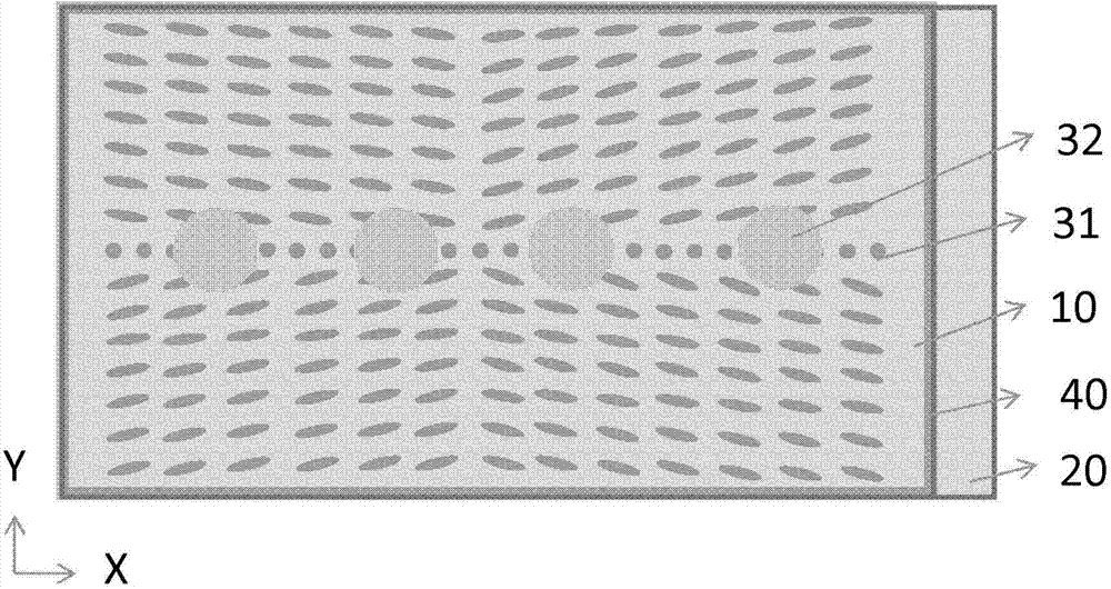
[0035] see figure 2 , the present invention provides a liquid crystal display panel, the liquid crystal display panel defines a long side defining a first direction X and a short side defining a second direction Y, wherein the length of the long side is greater than the length of the short side. like figure 2 As shown, the liquid crystal display panel includes a first substrate 10, a second substrate 20, and a plurality of spacer materials 31 arranged between the first substrate 10 and the second substrate 20, wherein liquid crystal droplets 32 ar...


PUM


Abstract

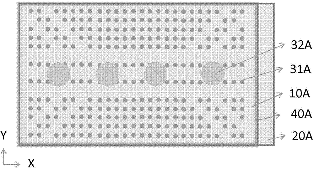
The invention provides a liquid crystal display panel. The liquid crystal display panel is provided with long edges for limiting a first direction and short sides for limiting a second direction, wherein the long sides are longer than the short sides. The liquid crystal display panel comprises a first substrate, a second substrate and a plurality of separating materials arranged between the first substrate and the second substrate, liquid crystal drops flow among the separating materials, and the arrangement density of the separating materials in the first direction is smaller than the arrangement density of the separating materials in the second direction. According to the liquid crystal display panel, contamination on the periphery of a small TFT-LCD device can be reduced, and it can be facilitated that the liquid crystal drops flow and diffuse to the corners of the small TFT-LCD device. Meanwhile, the invention further provides a manufacturing method for the liquid crystal display panel and a liquid crystal display device including the liquid crystal display panel.

Description

technical field [0001] The invention relates to the field of liquid crystal display technology, in particular to a liquid crystal display panel, a manufacturing method thereof, and a liquid crystal display device. Background technique [0002] In the field of liquid crystal display technology, there is a huge market demand for small-sized products such as mobile phones and Pads. In existing small-sized TFT-LCD devices, a one-line liquid crystal layout pattern design is usually adopted. like figure 1 The TFT liquid crystal display panel shown includes a CF substrate 1, a TFT substrate 2, and a plurality of spacer materials 3 formed between the CF substrate 1 and the TFT substrate 2, wherein liquid crystal droplets 5 are filled between the CF substrate 1 and the TFT substrate 2 and can flow between the plurality of spacer materials 3 . In addition, the peripheries of the CF substrate 1 and the TFT substrate 2 are sealed by a sealant 5 . However, in this liquid crystal patt...

Claims


Application Information

Patent Timeline
Patent Type & Authority Applications(China)
IPC IPC(8): G02F1/1339G02F1/1333
CPCG02F1/13394G02F1/13396G02F1/13415G02F1/13398
Inventor 张军
Owner HEFEI BOE OPTOELECTRONIC TECH CO LTD
Learn More