Trench type split-gate power device and manufacturing method thereof

A manufacturing method and technology for power devices, which are applied in semiconductor/solid-state device manufacturing, semiconductor devices, electrical components, etc., can solve the problem of large cross-sectional area of ​​split gate grooves, complicated manufacturing process, increased device on-resistance and power consumption, etc. problem, to achieve the effect of reducing cross-sectional area, reducing complexity, and reducing on-resistance

Active Publication Date: 2015-07-15
FUDAN UNIV
View PDF6 Cites 13 Cited by
  • Summary
  • Abstract
  • Description
  • Claims
  • Application Information

AI Technical Summary

Problems solved by technology

However, its manufacturing process is complicated, and the cross-sectional area occupied by the split gate groove is relatively large, which increases the on-resistance and power consumption of the device.

Method used


Image

  • Trench type split-gate power device and manufacturing method thereof
  • Trench type split-gate power device and manufacturing method thereof
  • Trench type split-gate power device and manufacturing method thereof

Examples


Embodiment Construction

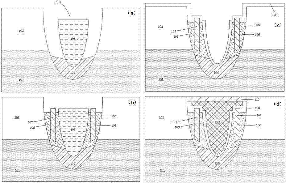
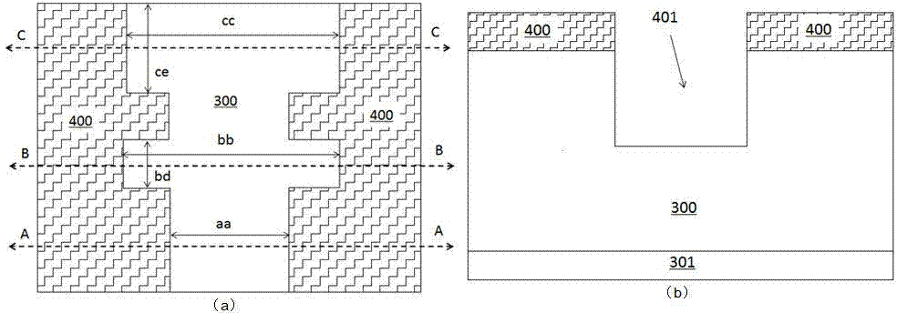
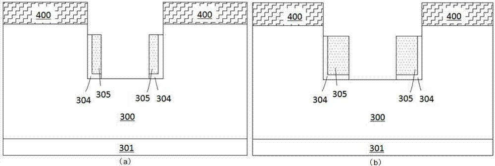
[0045] An exemplary embodiment of the present invention will be described in detail below with reference to the accompanying drawings. In the drawings, the thicknesses of layers and regions are exaggerated for convenience of illustration, and the shown sizes do not represent actual sizes. Although these figures do not completely reflect the actual size of the device, they still fully reflect the mutual positions between the regions and the constituent structures, especially the upper-lower and adjacent relationships between the constituent structures.

[0046]The referenced figures are schematic illustrations of idealized embodiments of the invention, and the illustrated embodiments of the invention should not be construed as limited to the particular shapes of regions illustrated in the figures but are to include resulting shapes, such as manufacturing-induced deviations. Also in the following description, the terms wafer and substrate used may be understood to include the se...


PUM


Abstract

The invention belongs to the technical field of semiconductor devices and particularly relates to a trench type split-gate power device and a manufacturing method thereof. According to the manufacturing method of the trench type split-gate power device, a control gate trench and a control gate are etched firstly, a substrate epitaxial layer is etched with a self-aligning manner to form a split-gate trench, and a split gate is formed in the split-gate trench. According to the method, the same mask is used for graphics of the control gate trench and the split-gate trench, the split-gate trench is etched with a self-aligning process, and the processing complexity of the device can be reduced; stray capacitance between the control gate and a drain region can be reduced, dynamic power consumption of the device is reduced, and the switching speed is increased; the cross-sectional area occupied by the split-gate trench can be reduced, and the on resistance of a chip is reduced.

Description

technical field [0001] The invention belongs to the technical field of semiconductor power devices, and in particular relates to a semiconductor power device and a manufacturing method thereof. Background technique [0002] With the continuous development of microelectronics technology, semiconductor power devices have high input impedance, low loss, fast switching speed, no secondary breakdown, wide safe working area, good dynamic performance, and easy coupling with the front electrode to achieve high current, With the advantages of high conversion efficiency, gradually replacing bipolar devices has become the mainstream of power device development today. Current semiconductor power devices mainly include planar power devices and trench power devices. [0003] Because the trench power device uses a vertical channel, the side wall of the channel can be used as a control gate, which occupies a smaller area than the planar power device, which can further increase the area of ...

Claims


Application Information

Patent Timeline
Patent Type & Authority Applications(China)
IPC IPC(8): H01L21/336H01L21/28H01L29/78H01L29/423
CPCH01L21/28H01L29/4232H01L29/66477H01L29/78
Inventor 王鹏飞
Owner FUDAN UNIV
Why Eureka
Try Eureka