Supercharge Your Innovation With Domain-Expert AI Agents!

Method for manufacturing flash memory

A manufacturing method and flash memory technology, applied in the field of flash memory manufacturing, can solve the problems of easy etching, semiconductor substrate 10 damage, narrow process window, etc., and achieve the effects of easy control of etching, improvement of yield rate, and avoidance of damage

Active Publication Date: 2015-07-15
SEMICON MFG INT (SHANGHAI) CORP
View PDF3 Cites 2 Cited by
  • Summary
  • Abstract
  • Description
  • Claims
  • Application Information

AI Technical Summary

Problems solved by technology

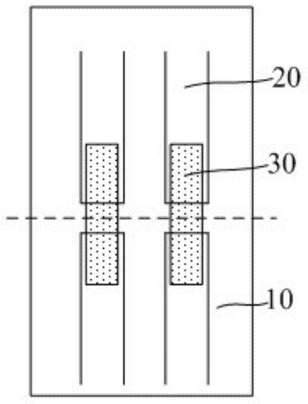
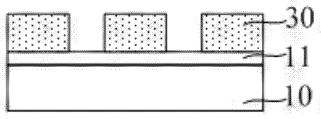
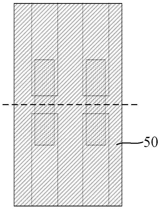
[0008] However, in step S4, when the control gate 50, the dielectric layer 40, and the floating gate 30 located on the surface of the oxide layer 11, the surface of the entire control gate 50 is uneven, and there is only one layer of control gate 50 in some areas, therefore , the degree of etching cannot be accurately controlled during etching. If the degree of etching is insufficient (Under Etch), residues 60 are likely to be left on the surface of the oxide layer 11, such as Figure 3b As shown; if the etching degree is relatively deep (Over Etch), because the oxide layer 11 is thin, it is usually very easy to be etched away, thereby causing damage to the semiconductor substrate 10
[0009] In summary, the flash memory manufacturing method in the prior art has a narrow process window and cannot meet the needs of the process.

Method used


Image

  • Method for manufacturing flash memory
  • Method for manufacturing flash memory
  • Method for manufacturing flash memory

Examples


Embodiment Construction

[0032] The method for manufacturing the flash memory of the present invention will be described in more detail below in conjunction with the schematic diagram, which shows the preferred embodiment of the present invention. It should be understood that those skilled in the art can modify the present invention described here and still achieve the advantageous effects of the present invention. Therefore, the following description should be understood to be widely known to those skilled in the art, and not as a limitation to the present invention.

[0033] For the sake of clarity, not all features of actual embodiments are described. In the following description, well-known functions and structures are not described in detail because they may confuse the present invention due to unnecessary details. It should be considered that in the development of any actual embodiment, a large number of implementation details must be made to achieve the developer's specific goal, such as changing ...


PUM


Abstract

The invention provides a method for manufacturing a flash memory. A floating gate is formed only on the surfaces of shallow trench isolations, and is no longer across the surfaces of the shallow trench isolations and an oxide layer. In the subsequent etching of a control gate, the floating gate does not need to be etched. Therefore, the etched layer is highly uniform, etching is easy to control, damage to or residue on a semiconductor substrate is avoided, and the yield of the flash memory is improved.

Description

Technical field [0001] The present invention relates to the field of semiconductor manufacturing, in particular to a method for manufacturing a flash memory. Background technique [0002] As a major non-volatile memory, flash memory has a wide range of uses in smart cards, microcontrollers and other fields. [0003] Please refer to Figure 1a to Figure 3a with Figure 1b to Figure 3b , Figure 1a to Figure 3a Is a top view of the flash memory manufacturing process in the prior art, Figure 1b to Figure 3b for Figure 1a to Figure 3b A schematic cross-sectional view along the dotted line; the flash memory manufacturing method in the prior art includes: [0004] S1: A semiconductor substrate 10 is provided. A shallow trench isolation (STI) 20 is formed in the semiconductor substrate 10, and an oxide layer 11 is formed on the surface of the semiconductor 10, such as Figure 1a with Figure 1b Shown [0005] S2: A strip-shaped floating gate (FG) 30 is formed on the surface of the shallow tr...

Claims


Application Information

Patent Timeline
Patent Type & Authority Applications(China)
IPC IPC(8): H01L21/8247H01L21/28H10B41/35
CPCH01L29/42324H01L29/66825H10B69/00
Inventor 张冬平万宇
Owner SEMICON MFG INT (SHANGHAI) CORP
Features
  • R&D
  • Intellectual Property
  • Life Sciences
  • Materials
  • Tech Scout
  • Unparalleled Data Quality
  • Higher Quality Content
  • 60% Fewer Hallucinations
Learn More