
Low frequency surface plasmon waveguide structure

A surface plasmon and waveguide structure technology, applied in waveguides, waveguide-type devices, circuits, etc., can solve problems such as poor constraints, inability to effectively concentrate electromagnetic waves, and inability to achieve better distribution of electromagnetic fields, and the distribution of electromagnetic fields is easy to control. , the effect of effective constraints

Inactive Publication Date: 2017-08-04
CHUNG HUA UNIVERSITY
View PDF4 Cites 0 Cited by
  • Summary
  • Abstract
  • Description
  • Claims
  • Application Information

AI Technical Summary

Problems solved by technology

[0004] Generally, the surface plasmon frequency of metals is in the ultraviolet band, so the performance of metals in the terahertz band is approximately an ideal conductor (Perfect Electric Conductor, PEC), which makes SPPs on the metal surface poorly bound to the electromagnetic field and cannot effectively concentrate electromagnetic waves. This limits the application of leaky-wave antennas with general structures in the terahertz and microwave bands
[0005] However, due to the situation of surface plasmon modes, it cannot be realized at low frequencies such as microwave and terahertz (THz) bands.

Method used


Image

  • Low frequency surface plasmon waveguide structure
  • Low frequency surface plasmon waveguide structure
  • Low frequency surface plasmon waveguide structure

Examples


Embodiment Construction

[0054] The specific technology adopted in the present invention will be further described through the following examples and attached drawings.

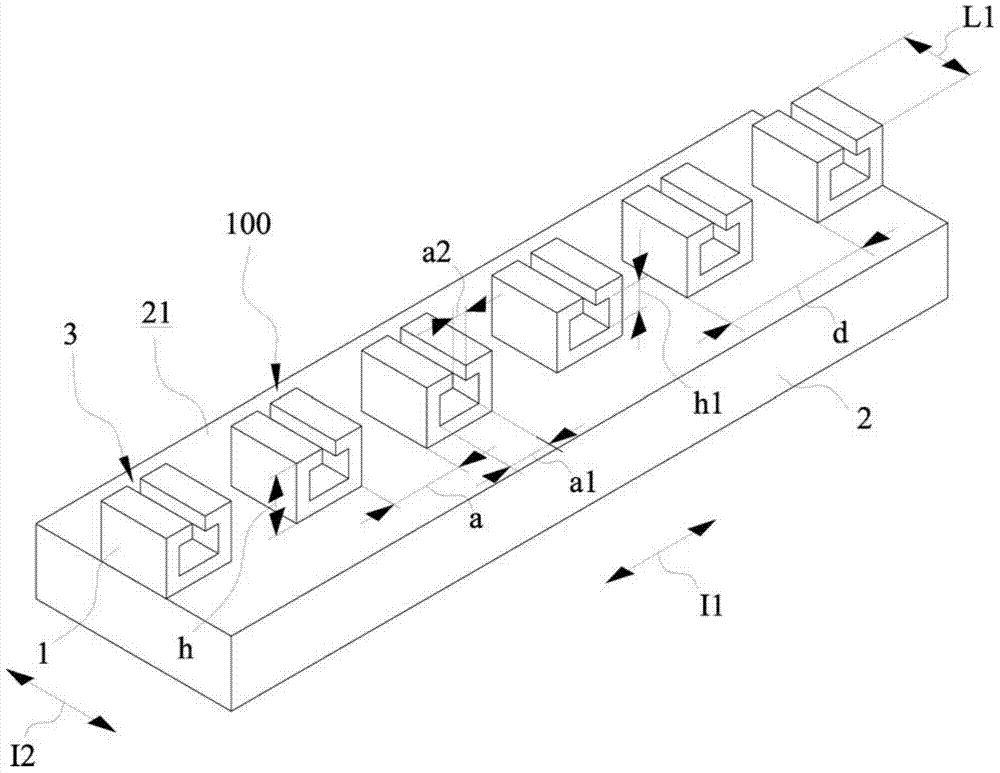
[0055] see figure 1 , which shows a perspective view of the low-frequency surface plasmon waveguide structure of the first embodiment of the present invention. The low-frequency surface plasmon waveguide structure of the present invention includes a plurality of unit cell blocks 1 arranged at a predetermined distance from each other on the upper surface 21 of a flat metal substrate 2 . Each unit cell block 1 is arranged in a straight line on the upper surface 21 of the metal substrate 2 along the one-dimensional arrangement direction I1 at a subwavelength period (subwave length periodic) to form a hollow metal block periodic structure 100 (metallic hollow blocks periodic structure ).

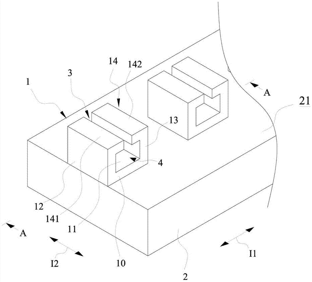
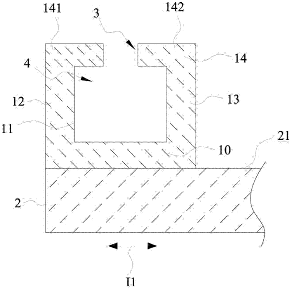
[0056] refer to Figure 2-Figure 3 , are respectively an enlarged perspective view and a cross-sectional view of the specific embodiment of the uni...


PUM


Abstract

Provided is a low-frequency surface plasma waveguide structure. Multiple single-cell blocks are arranged along a one-dimensional arrangement direction in a sub wavelength periodic manner to form a metallic hollow block periodic structure. Each single-cell block comprises a substrate, a penetrating part, and an open slot. Each penetrating part is formed in the corresponding single-shell block in a penetrating direction perpendicular to the one-dimensional arrangement direction to define a groove space in the single-cell block. In a low-frequency spoof surface plasmon polariton transmission mode, the electromagnetic field distribution of each single-cell block is mostly limited in the groove space of the single-cell block if the structure is used as a structure of the antenna, and most of the electromagnetic fields are distributed between two adjacent single-cell blocks and a few is distributed in the grooves if the structure is used for waveguide. By adopting the low-frequency surface plasma waveguide structure of the invention, an electromagnetic field can be constrained more highly, and a better transmission effect can be achieved compared with a metallic solid block periodic structure array waveguide.

Description

technical field [0001] The invention relates to a low-frequency surface plasmon waveguide structure, in particular to a new type of leaky waveguide composed of a special hollow metal square periodic structure surface, so that the metal surface can transmit electromagnetic waves more efficiently, and can be used as a Components with highly directional radiation. Background technique [0002] The concept of surface plasmons can be used to manipulate electromagnetic waves so that they can be transmitted in sub-wavelength lines, which is an important topic for effectively improving the device density in photonic circuit systems and integrated circuits. Surface plasmon polaritons (Surface Plasmon Polaritons, SPPs) are a mixed excited state of electrons and photons at the interface between a metal and a medium (usually air). decays exponentially with the medium. SPPs can offer the possibility of guiding electromagnetic waves beyond the diffraction limit, and thus have attracted ...

Claims


Application Information

Patent Timeline
Patent Type & Authority Patents(China)
IPC IPC(8): H01P3/12
Inventor 吴家和
Owner CHUNG HUA UNIVERSITY
Learn More