Supercharge Your Innovation With Domain-Expert AI Agents!

Integrated circuit chip subjected to modularized packaging and manufacturing method thereof

A technology of integrated circuits and manufacturing methods, which is applied in the direction of circuits, electrical components, and electrical solid devices, can solve problems such as high cost of upgrading, failure to realize effective utilization of bare chips, and non-uniform interfaces of bare chips, and achieve convenient and reliable replacement. Good scope of application and low development risk

Active Publication Date: 2015-07-22
宁波中控微电子有限公司
View PDF4 Cites 3 Cited by
  • Summary
  • Abstract
  • Description
  • Claims
  • Application Information

AI Technical Summary

Problems solved by technology

[0004] System-in-package technology has many advantages, especially in quickly completing the research and development of chip products. The original die cannot be replaced directly when updating and upgrading
At present, when the chip needs to be upgraded, only the whole chip can be replaced, which results in more chip design time and prolongs the time required for product upgrades
Moreover, the replaced chip also caused a waste of resources, and did not realize the effective utilization of the bare chip.
The impact of the above time delays and waste of resources will be significant when upgrading chips for high-volume products
[0005] To sum up, the current common chip system-in-package methods generally have the problems of narrow application range, low plasticity, and high upgrade cost.

Method used


Image

  • Integrated circuit chip subjected to modularized packaging and manufacturing method thereof
  • Integrated circuit chip subjected to modularized packaging and manufacturing method thereof
  • Integrated circuit chip subjected to modularized packaging and manufacturing method thereof

Examples


Embodiment Construction

[0034] The present invention will be described in detail below in terms of specific embodiments in conjunction with the accompanying drawings. The following examples will help those skilled in the art to further understand the present invention, but do not limit the present invention in any form. It is to be noted that other embodiments may be utilized or structural and functional modifications may be made to the embodiments set forth herein without departing from the scope and spirit of the invention.

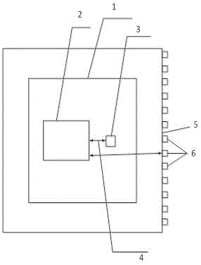
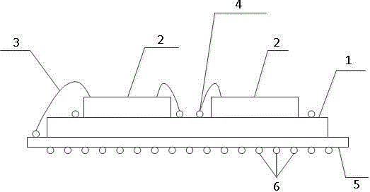
[0035] Such as figure 1 As shown, a common system-in-package chip in the prior art generally includes a first die 1, a second die 2, a bridge interface 3, a bridge circuit 4, a substrate 5 for placing the first die, and chip pins 6 . The second die 2 is located above the first die 1 , the substrate 5 is located below the first die 1 , and the chip pins 6 are led out from the first die 1 and / or the second die 2 and extend to the substrate 5 outside. The bridge interface 3 i...


PUM


Abstract

The invention provides an integrated circuit chip subjected to modularized packaging and a manufacturing method thereof, the method comprises: S1, a plurality of first bare chips and a plurality of second bare chips are manufactured according to the requirements of functions and properties of a target chip, the shapes of the first bare chips and second bare chips are squares and rectangles consisting of an integral number of preset benchmark rectangles, the second bare chips are less than the first bare chips, the first bare chips are provided with a plurality of interfaces between which preset intervals are arranged, the interfaces form an interface matrix, the number of the interfaces is greater than that of the manufactured second bare chips, and the preset intervals are greater than the maximum sizes of the second bare chips; S2, a first bare chip and at least one second bare chip are selected from the plurality of first bare chips and the plurality of second bare chips which are manufactured from the S1; S3, modularized packaging is carried out on the first bare chips and the second bare chips which are selected from the S2 so as to obtain the target chips.

Description

technical field [0001] The invention relates to the field of system-in-package manufacturing, in particular to a modular packaged integrated circuit chip and a manufacturing method thereof. Background technique [0002] With the continuous development of the chip manufacturing process, the continuous improvement of the integration level, and the increasingly complex functions of the chip, the difficulty of chip design is also increasing day by day. The SiP (System in Package, system-in-package) technology that combines mature bare chips into a chip is an emerging technology that emerged as the times require. This technology refers to the integration of bare chips with multiple functions (including central processing unit, coprocessor, memory, resistors, capacitors, inductors, etc.) into one package according to needs, and finally realizes complete functions. It should be pointed out that SiP is similar to SoC (System on a Chip), but SiP uses different chips to be packaged s...

Claims


Application Information

Patent Timeline
Patent Type & Authority Applications(China)
IPC IPC(8): H01L21/50H01L21/60H01L25/00
CPCH01L25/00H01L21/50H01L2924/15311H01L2224/48091H01L2224/48137H01L2224/48464H01L2924/00014
Inventor 沈天扬施一明潘再生王挺童庆唐艳丽朱冬冬方科科王建平
Owner 宁波中控微电子有限公司
Features
  • R&D
  • Intellectual Property
  • Life Sciences
  • Materials
  • Tech Scout
  • Unparalleled Data Quality
  • Higher Quality Content
  • 60% Fewer Hallucinations
Learn More