Supercharge Your Innovation With Domain-Expert AI Agents!

Semiconductor packaging structure and semiconductor technology

A packaging structure and semiconductor technology, applied in semiconductor devices, semiconductor/solid-state device manufacturing, semiconductor/solid-state device components, etc., can solve the problems of increased packaging costs and high cost of copper core solder balls

Active Publication Date: 2015-07-22
ADVANCED SEMICON ENG INC
View PDF5 Cites 0 Cited by
  • Summary
  • Abstract
  • Description
  • Claims
  • Application Information

AI Technical Summary

Problems solved by technology

However, the cost of the copper core solder ball is higher than that of the solder ball, resulting in an increase in packaging cost

Method used


Image

  • Semiconductor packaging structure and semiconductor technology
  • Semiconductor packaging structure and semiconductor technology
  • Semiconductor packaging structure and semiconductor technology

Examples


Embodiment Construction

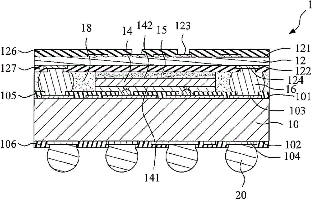
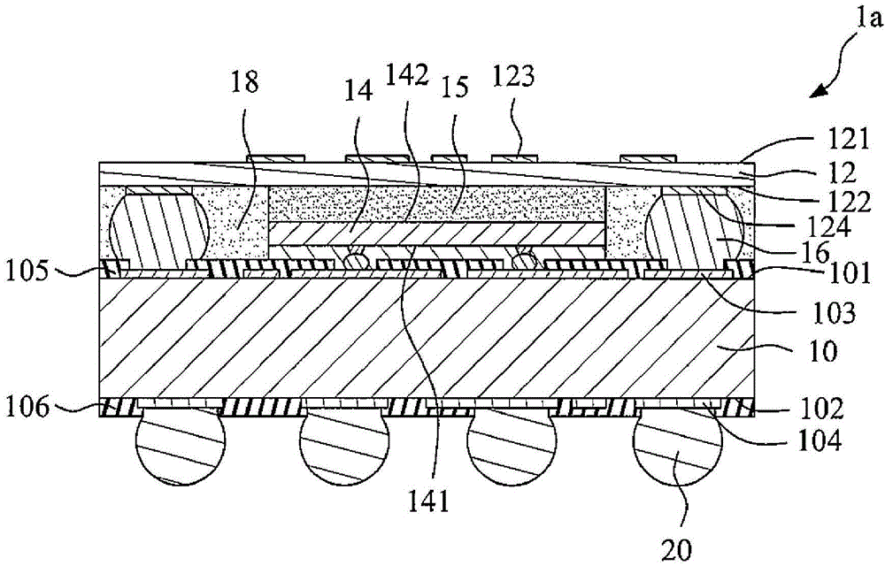
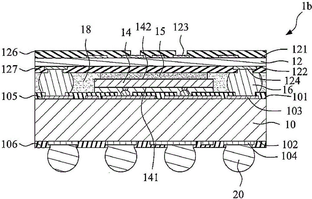
[0012] refer to figure 1 , shows a schematic cross-sectional view of an embodiment of the semiconductor package structure of the present invention. The semiconductor package structure 1 includes a first substrate 10 , a second substrate 12 , a die 14 , an adhesive film 15 , a plurality of interconnection elements 16 , a cladding material 18 and a plurality of lower solder balls 20 .

[0013] The first substrate 10 has an upper surface 101 , a lower surface 102 , a plurality of conductive pads 103 on the first substrate and a plurality of conductive pads 104 under the first substrate. In this embodiment, the first substrate 10 is a packaging substrate, the conductive pad 104 under the first substrate is exposed on the lower surface 102 of the first substrate 10, and the conductive pad 104 on the first substrate Pads 103 are exposed on the upper surface 101 of the first substrate 10 . The conductive pad 104 under the first substrate is electrically connected to the conductive ...


PUM

PropertyMeasurementUnit
Particle sizeaaaaaaaaaa

Abstract

The invention relates to a semiconductor packaging structure and semiconductor technology. the semiconductor packaging structure comprises a first substrate, a second substrate, a bare die, multiple inner connection elements, an adhesive film and a coating material, wherein the bare die is electrically connected with the first substrate; the inner connection elements are connected with the first substrate and the second substrate; the adhesive film is bonded on the second substrate and the bare die; the adhesive film is formed by a sheet film; and the coating material is located between the upper surface of the first substrate and the lower surface of the second substrate so as to coat the bare die, the adhesive film and the inner connection elements.

Description

technical field [0001] The invention relates to a semiconductor package structure and a semiconductor process. Specifically, the present invention relates to a stacked semiconductor package structure and semiconductor process thereof. Background technique [0002] The fabrication method of a conventional stacked semiconductor package structure is as follows. First, a die is bonded to the upper surface of a lower substrate. Next, an upper substrate is placed, and the upper substrate has a plurality of solder balls to be electrically connected to the upper surface of the lower substrate. Afterwards, a molding process is performed to form a sealing material between the upper and lower substrates. However, in this way, the solder balls need to be used as height control between the upper and lower substrates, so the solder balls need to use copper core tin balls to prevent the solder balls from melting due to solder balls. Lack of support leads to collapse. However, the cost ...

Claims


Application Information

Patent Timeline
IPC IPC(8): H01L23/31H01L23/48H01L21/56H01L21/60
CPCH01L2224/16225H01L2224/32225H01L2224/73204H01L2224/73253H01L2924/15311H01L2924/15331H01L2924/00
Inventor 王维仁张维刚庄翊钧
Owner ADVANCED SEMICON ENG INC
Features
  • R&D
  • Intellectual Property
  • Life Sciences
  • Materials
  • Tech Scout
  • Unparalleled Data Quality
  • Higher Quality Content
  • 60% Fewer Hallucinations
Learn More