Method for planning interlocking micro-bump matrix of overlapped type three-dimensional integrated chips
An integrated chip and three-dimensional integration technology, which is applied in special data processing applications, instruments, electrical digital data processing, etc., can solve the problems that are difficult to meet Moore's Law, and achieve the effects of strong intuition, short running time, and high accuracy
- Summary
- Abstract
- Description
- Claims
- Application Information
AI Technical Summary
Problems solved by technology
Method used
Image

Examples
Embodiment Construction
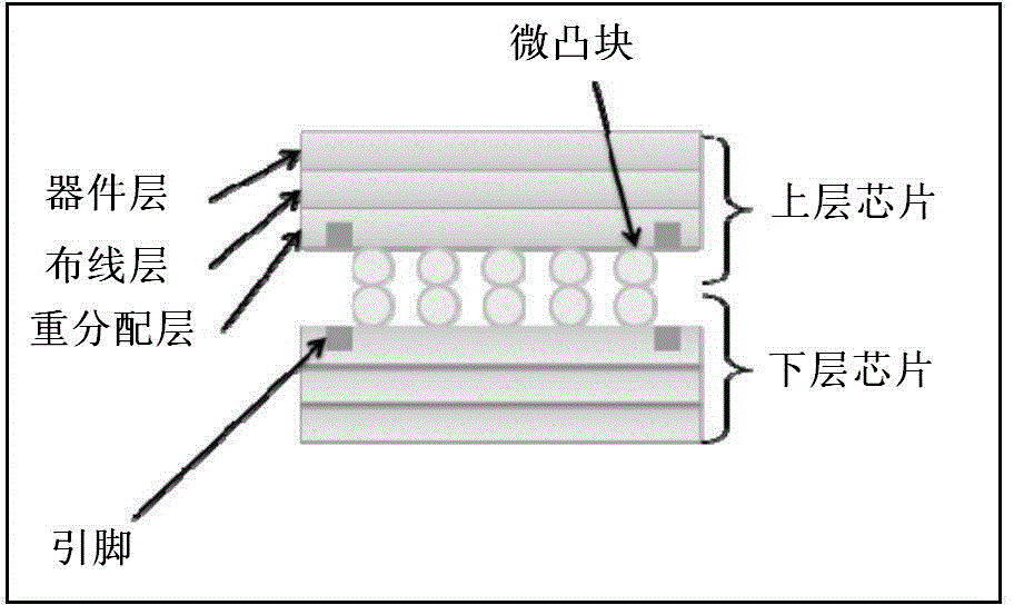
[0042] In the three-dimensional design, the micro-bump technology plays an auxiliary role in the connection of the upper and lower pins. The present invention can connect the micro-bumps of the middle layer to the pins for different initial chip states. cross each other.
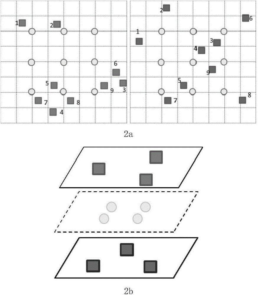
[0043] In order to make the problem concise, we transform the three-dimensional problem into a two-dimensional problem to solve.
[0044] The method for planning the matrix of micro-bumps interconnected between stacked three-dimensional integrated chips is characterized in that it is implemented in the computer according to the following steps in sequence:
[0045] Step (1), initialization, given an n, n represents the number of pin pairs, and the total number of pins is 2n. The coordinates of these 2n points are generated by simulation with random numbers. Each coordinate is an integer in the interval [0,100]. The chip is considered as a standard square with a side length of 100.
[0046] Let m be the ...
PUM
 Abstract
Description
Claims
Application Information