Waveguide structure, waveguide coupling structure, and preparation method
A technology of waveguide structure and silicon waveguide, which is applied in the direction of light guide, optics, instrument, etc., can solve the problems of large refractive index difference of silicon waveguide, high temperature sensitivity of silicon-based arrayed waveguide grating, no athermal solution, etc.
- Summary
- Abstract
- Description
- Claims
- Application Information
AI Technical Summary
Problems solved by technology
Method used
Image

Examples
Embodiment 1
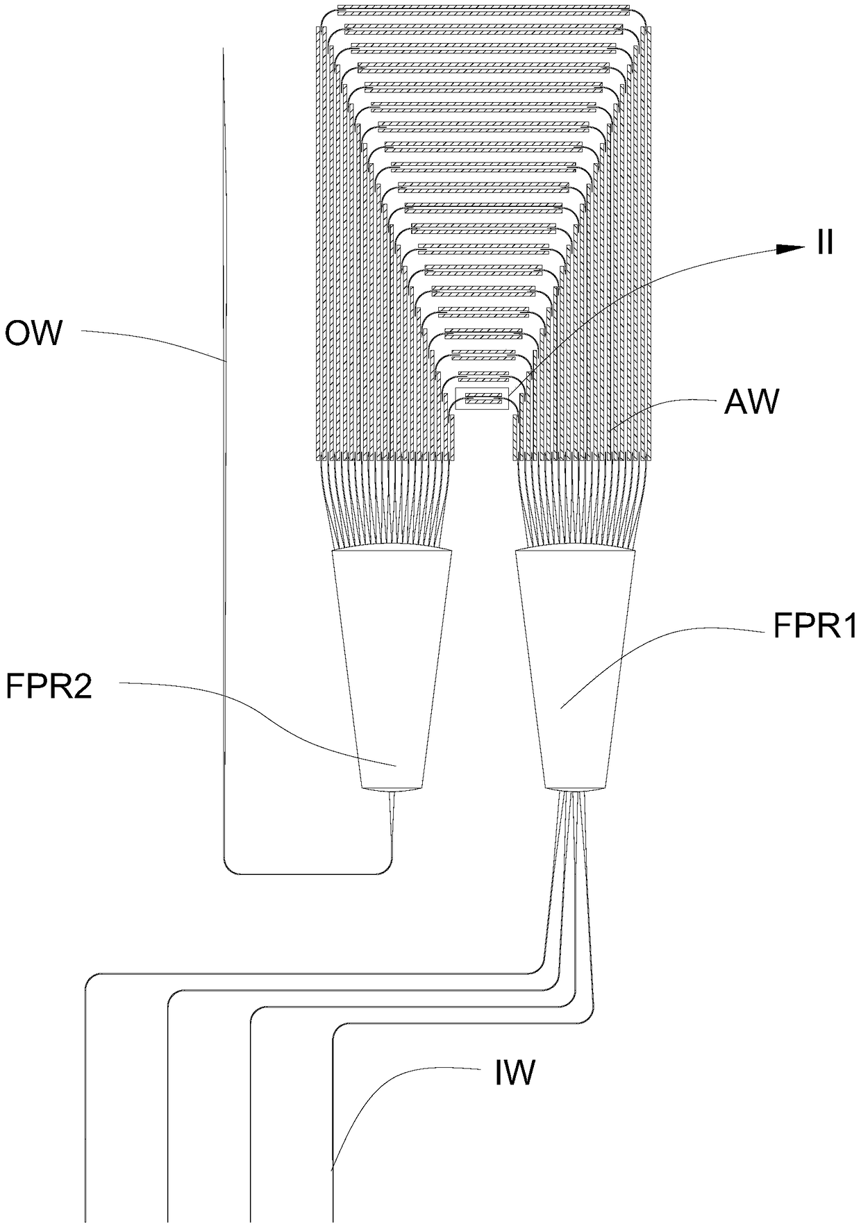
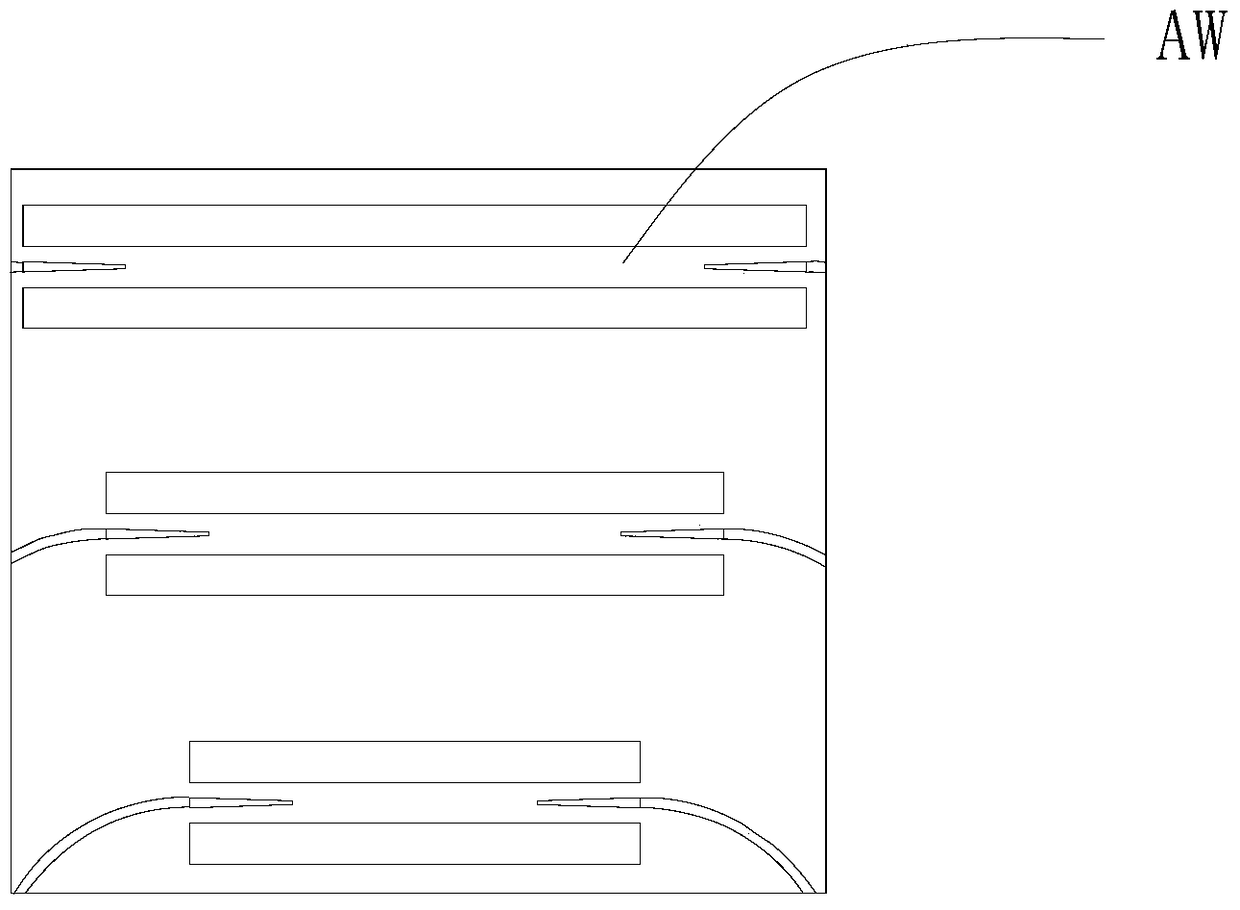
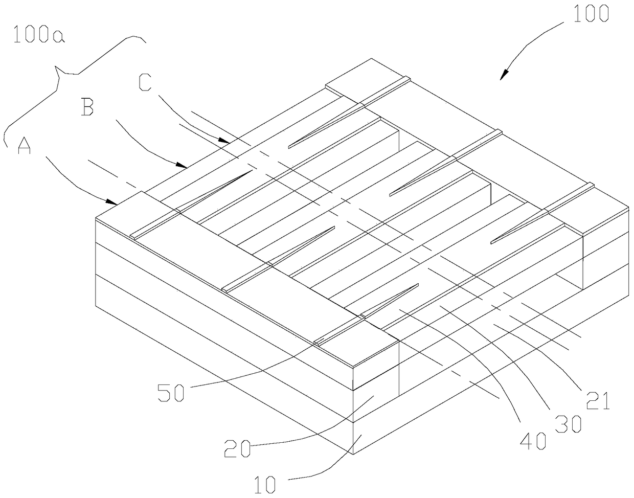
[0080] see image 3 , is a schematic diagram of the waveguide structure 100 provided by the present invention, the waveguide structure is protruding, the waveguide structure is applied to the straight waveguide part of the arrayed waveguide AW in the SOI-based arrayed waveguide grating, and the waveguide structure 100 adopts SOI crystal The silica in the circle serves as the lower cladding.
[0081]The waveguide structure 100 includes two first end portions 100a arranged axially symmetrically. The first end portion 100a is sequentially divided into a first area A, a second area B and a third area C along a direction close to the axis of symmetry. The waveguide structure 100 includes a first silicon substrate layer 10 , a second silicon substrate layer 20 , a first silicon dioxide layer 30 , a second silicon dioxide layer 40 and a first silicon waveguide layer 50 .
[0082] Comprehensive reference image 3 and Figure 4 , in the first region A, the first silicon substrate l...
Embodiment 2
[0097] see Figure 8 , is a structural schematic diagram of the waveguide structure 200 provided by the present invention, the waveguide structure 200 is buried, and the waveguide structure 200 is applied to the straight waveguide part of the arrayed waveguide AW in the SOI-based arrayed waveguide grating. The waveguide structure 200 adopts a structure in which a low refractive index waveguide layer is added on the surface of silicon photonics.
[0098] The waveguide structure 200 includes two first end portions 200a arranged axially symmetrically. The first end portion 200a is divided into a first region D, a second region E and a third region F along a direction close to the axis of symmetry. The waveguide structure 200 includes a third silicon substrate layer 110 , a third silicon dioxide layer 120 , a second silicon waveguide layer 130 , a first waveguide layer 140 and a second waveguide layer 150 stacked in sequence. The coverage area of the second silicon waveguide l...
Embodiment 3
[0113] see Figure 13 , the present invention also discloses the application of the waveguide coupling structure 300 provided in Embodiment 1, and the waveguide coupling structure is used in a mode-spot converter for coupling a silicon waveguide and a laser source. The structure of the waveguide coupling structure 300 in this embodiment is roughly the same as that of the waveguide structure 100 in Embodiment 1, the difference is that the waveguide coupling structure 300 is only half of the structure of the waveguide structure 100 . And, it is coupled with the laser source in the third region I.
[0114] The waveguide coupling structure 300 is divided into a first region G, a second region H and a third region I along a direction close to the laser source. The waveguide coupling structure 300 includes a fourth silicon substrate layer 310 , a fifth silicon substrate layer 320 , a fourth silicon dioxide layer 330 , a fifth silicon dioxide layer 340 and a third silicon waveguide...
PUM
 Abstract
Description
Claims
Application Information
 - R&D Engineer
- R&D Manager
- IP Professional
- Industry Leading Data Capabilities
- Powerful AI technology
- Patent DNA Extraction
Browse by: Latest US Patents, China's latest patents, Technical Efficacy Thesaurus, Application Domain, Technology Topic.
© 2024 PatSnap. All rights reserved.Legal|Privacy policy|Modern Slavery Act Transparency Statement|Sitemap