FPGA-based video synchronous switching system and method
A video synchronization and switching system technology, applied in the field of signal processing, can solve the problems of reduced image quality, large video channel delay, and low integration, and achieve the effect of over-extending image lines, simple circuits, and high integration
- Summary
- Abstract
- Description
- Claims
- Application Information
AI Technical Summary
Problems solved by technology
Method used
Image
Examples
Embodiment 1
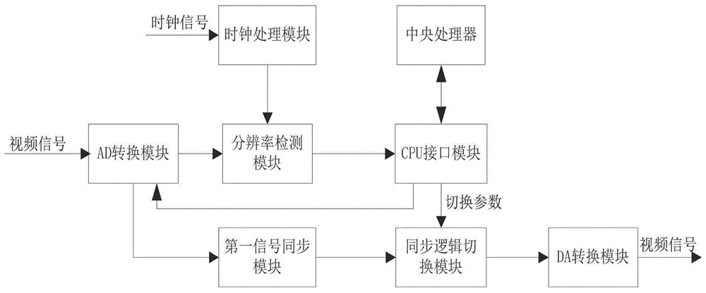
[0055] Such as Figure 7 The schematic diagram of a specific embodiment of the present invention shown, the multi-channel analog video signal is converted into the multi-channel digital video signal through the AD conversion module, and the high-speed detection clock that the resolution detection module produces with the clock processing module is to the multi-channel output of the AD conversion module The channel digital video signal is sampled, and the collected relevant parameters are submitted to the central processing unit through the CPU interface module. The central processing unit sets the AD conversion module according to the corresponding parameters, and receives and transmits the external switching finger parameters.
[0056] The first signal synchronization module performs multi-level synchronization on multi-channel digital video signals by inserting multi-level registers on the signal transmission path, reduces the line delay between registers, improves the operat...
Embodiment 2
[0061] This embodiment is based on the arbitrary synchronous switching output of 5-way VGA video input to 4-way VGA video.
[0062] Such as Figure 8 The schematic block diagram of another specific embodiment is shown, 5 channels of VGA video signals are input, and converted into digital video information in RGB888 color mode by an AD decoding chip. Since the VGA decoding chip cannot determine the effective area of the video output, the effective area of the output needs to be set by the central processing unit. If the central processing unit does not know its resolution, the effective area of the video output will be deviated. As a result, when the monitor outputs, it will cause black borders to appear in the video. The clock processing module multiplies the frequency of the external input clock to generate the high-speed detection clock required by the VGA resolution detection module. The clock logic module can also eliminate duty cycle distortion of the external inp...
PUM
 Abstract
Description
Claims
Application Information


