Supercharge Your Innovation With Domain-Expert AI Agents!

A boost circuit device based on disturbance observation

A technology of circuit device and disturbance observation, which is applied in the field of nonlinear factors and disturbance theory and circuit realization, can solve problems such as input voltage fluctuation, output voltage accuracy is difficult to guarantee, and transfer function cannot be directly obtained, so as to reduce output Voltage steady-state error, the effect of improving the output voltage stability ability

Inactive Publication Date: 2017-05-03
JIANGSU UNIV
View PDF3 Cites 0 Cited by
  • Summary
  • Abstract
  • Description
  • Claims
  • Application Information

AI Technical Summary

Problems solved by technology

[0005] Due to nonlinear and non-minimum phase problems in the mathematical model of the Boost converter, its transfer function cannot be obtained directly
At the same time, due to problems such as model perturbation, input voltage fluctuations and load changes in the system, it is difficult to guarantee the accuracy of the output voltage

Method used


Image

  • A boost circuit device based on disturbance observation
  • A boost circuit device based on disturbance observation
  • A boost circuit device based on disturbance observation

Examples


Embodiment 1

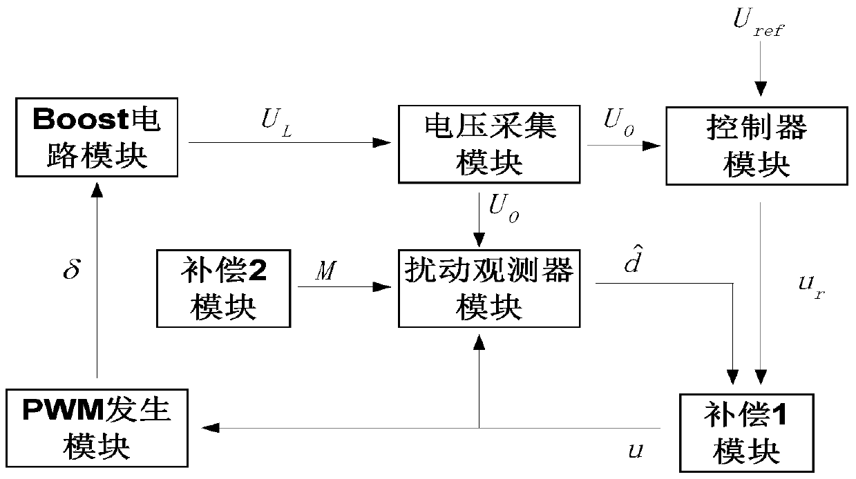
[0045] Circuit structure of the present invention is as follows:

[0046] The Boost circuit device based on disturbance observation includes: Boost circuit module, voltage acquisition module, controller module, compensation 1 module, compensation 2 module, PWM generation module and disturbance observer module;

[0047] The Boost circuit module is to connect the power supply V1, the inductor L, the diode D1 and the resistor R in series to form a loop, connect the drain D end of the MOSFET Q1 to the positive end of the diode D1, and connect the source S of the MOSFET Q1 Connect the negative end of the power supply V1 to the negative end of the power supply V1, connect one end of the capacitor C to one end of the resistor R1, connect the other end of the capacitor C to the negative end of the diode D1, and connect the other end of the resistor R1 to the power supply The negative terminal of V1 is connected.

[0048] The said voltage acquisition module connects the resistors R3 a...

Embodiment 2

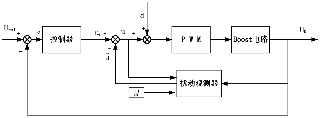
[0069] The working principle of the device of the present invention is:

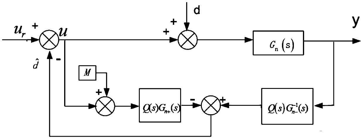
[0070] Figure 4 As shown in the schematic block diagram of the disturbance observer, the present invention selects the small signal transfer function of the Boost circuit as a nominal model, as follows:

[0071]

[0072] where U i is the input voltage at steady state, L, C and R are the inductance, capacitance and load respectively, D'=1-D, D is the value of the switch duty cycle at steady state, due to the non-minimum phase characteristic of the Boost circuit, Its transfer function cannot be obtained directly, and the present invention adopts the small signal transfer function of Boost circuit to replace its original transfer function through a series of transformations, and the small signal transfer function of Boost circuit has the following form:

[0073]

[0074] For the convenience of analysis, the small signal transfer function of the Boost circuit is here Simplifies to:

[0075]

...


PUM


Abstract

The invention discloses a Boost circuit device based on disturbance observation, which includes a Boost circuit module, a voltage acquisition module, a controller module, a compensation 1 module, a compensation 2 module, a disturbance observer module and a PWM generation module, and the compensation 1 module is used for The purpose is to use the disturbance value estimated by the disturbance observer module as the compensation amount to compensate the output signal of the controller module; the compensation 2 module is used to compensate the error between the observed value and the actual value of the disturbance. The Boost circuit device based on disturbance observation adopts a common control algorithm to design a feedback controller, combines the disturbance observer to observe the disturbance in the Boost, and uses the obtained disturbance estimation value as feed-forward compensation to the input terminal, and forms a feedback loop with the common control algorithm. Feed-forward composite control scheme. The method proposed by the invention does not need to change the original feedback controller, but also can significantly improve the control effect, and the design method is simple and easy to realize.

Description

technical field [0001] The invention relates to the control field of power electronic converters, and more specifically relates to a theoretical method and a realization circuit for eliminating nonlinear factors and interference of Boost circuits. Background technique [0002] In recent years, due to the development of power electronics technology, Boost converters are widely used in various DC Boost applications, such as photovoltaic power generation, laser power supply, electric and hybrid vehicles, LED lighting, and new energy grid-connected fields. However, due to the nonlinear and non-minimum phase characteristics in the mathematical model of the Boost converter, it brings great inconvenience to the design of the system control. In addition, when the nonlinear factors or disturbances in the system are large, it is very difficult to meet the high-precision voltage regulation control requirements under the action of the linear controller. [0003] It is worth noting that...

Claims


Application Information

Patent Timeline
Patent Type & Authority Patents(China)
IPC IPC(8): H02M3/156
CPCH02M3/155H02M1/0016
Inventor 马莉徐媚媚丁世宏王加典
Owner JIANGSU UNIV
Features
  • R&D
  • Intellectual Property
  • Life Sciences
  • Materials
  • Tech Scout
  • Unparalleled Data Quality
  • Higher Quality Content
  • 60% Fewer Hallucinations
Learn More