Multi-serial port extension method based on FPGA and TL16C554A
A technology of TL16C554A and expansion method, applied in the field of multi-serial port expansion, can solve the problems of loss of serial port sending and receiving data, low serial port reliability, and no consideration of serial port expansion chip timing drive, etc., and achieves high real-time performance, high reliability and flexibility. changing effect
- Summary
- Abstract
- Description
- Claims
- Application Information
AI Technical Summary
Problems solved by technology
Method used
Image
Examples
Embodiment 1
[0059] Technical indicators of this expansion method:
[0060] DSP processor: TMS320C6713B
[0061] FPGA: EP2C50F484I8
[0062] Serial expansion chip: TL16C554A
[0063] Serial port level conversion chip: MAX3490
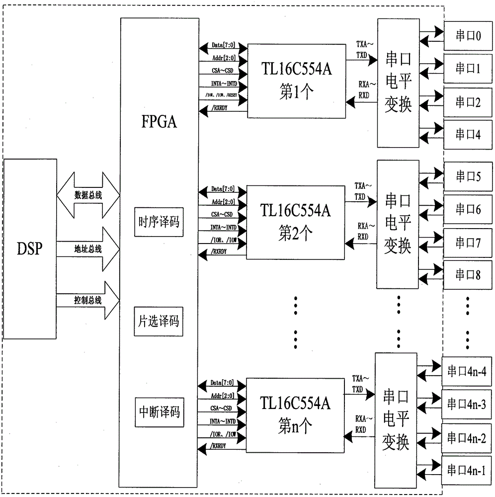
[0064] If the DSP processor TMS320C6713B is used in the multi-sensor real-time data acquisition system (here the processor is DSP as an example, other types of processors can choose the corresponding signal line, the same below), since the processor itself does not have a serial port, the serial port When the expansion chip expands multiple serial ports, the multi-serial port expansion method invented by this patent includes FPGA, TL16C554A, serial port level conversion chip, and the functional block diagram is as follows figure 1 shown.
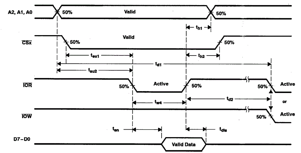
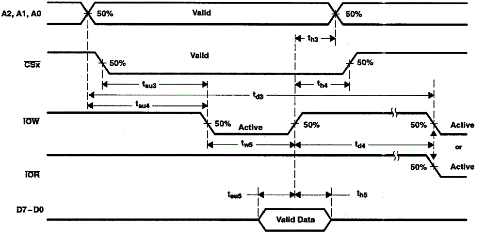
[0065]Among them, FPGA mainly completes the communication with DSP, as well as the timing drive, chip selection decoding and interrupt decoding of TL16C554A. TL16C554A is a management unit for asynchronous serial communicatio...
Embodiment 2
[0109] like Image 6 It is an implementation mode for expanding 32 serial ports outside the DSP processor. Among them, FPGA chooses EP2C50F484I8, which has 294 available IOs, which meets the 184 IOs required for the connection between 8 TL16C554A and FPGA and the 29 IOs required for the connection between DSP and FPGA. The clock frequency of the FPGA crystal oscillator is 40MHz.
[0110] FPGA occupies 5 double-byte addresses in the corresponding address space of DSP chip select signal CE3, 0xB0000000, 0xB0000002, 0xB0000004, 0xB0000006 and 0xB0000008, which are respectively used for the control word CTRL_WORD_C54 pointer, the sending data DATA_TO_C54 pointer, the receiving data DATA_FROM_C54 pointer, and two self- Define the interrupt flag register pointers C54_INT_REG0 and C54_INT_REG1. The FPGA completes the decoding of these three address pointers according to CE3, the lower 8-bit address line, the DSP read signal line, and the DSP write signal line, and reads data from t...
PUM
 Abstract
Description
Claims
Application Information


