OLED pixel circuit and display device thereof

A pixel circuit and electrode technology, which is applied in the field of OLED pixel circuits and display devices, can solve the problems of uneven light emission, inconsistent brightness of OLED devices, and unstable process, and achieve the effect of compensation for uneven light emission

Active Publication Date: 2015-09-09
BOE TECH GRP CO LTD
View PDF10 Cites 45 Cited by
  • Summary
  • Abstract
  • Description
  • Claims
  • Application Information

AI Technical Summary

Problems solved by technology

[0002] In the existing TFT-OLED pixel circuit, there are OLED current changes caused by uncontrollable factors such as process instability, parameter drift, and device aging of TFT and OLED light-emitting devices, which in turn leads to uneven light emission of the display panel.
[0003] In order to solve the problem of uneven luminescence, the existing electrical compensation methods usually use the detection

Method used


Image

  • OLED pixel circuit and display device thereof
  • OLED pixel circuit and display device thereof
  • OLED pixel circuit and display device thereof

Examples


Embodiment 1

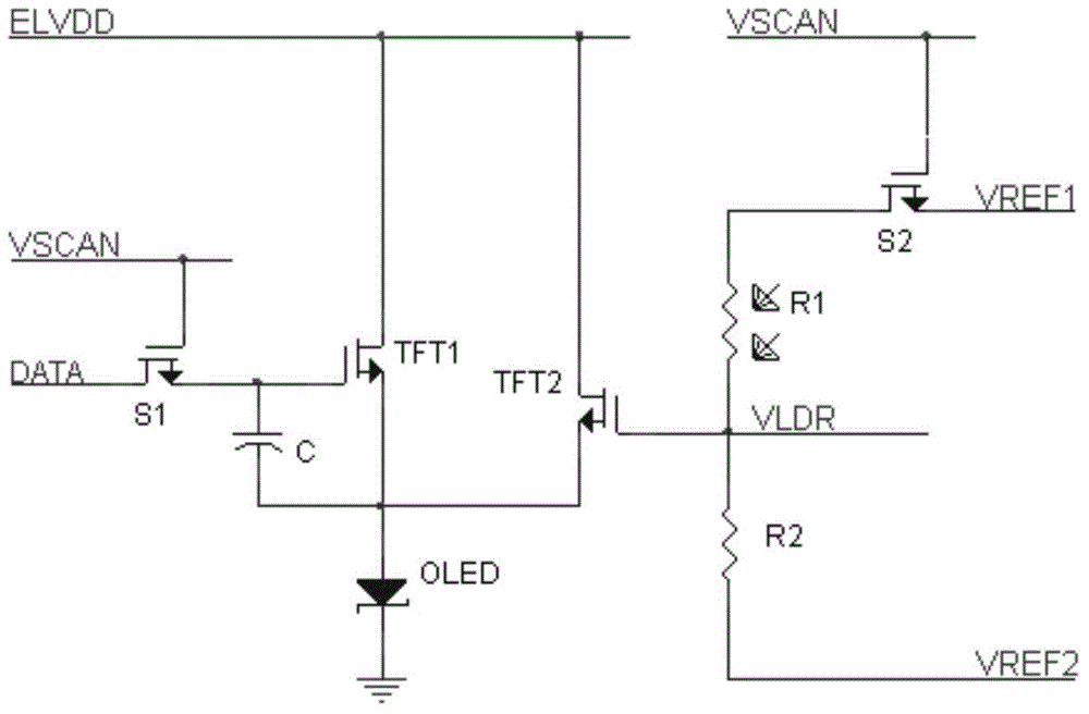
[0045] This embodiment provides an OLED pixel circuit, which uses a positive coefficient photoresistor to compensate the driving circuit of the N-type thin film transistor. The specific circuit structure is as follows: figure 1 , 2 shown.

[0046] In the OLED pixel circuit, the sensing element is a photoresistor, and the compensation unit also includes a synchronous transistor, a compensation drive tube and a voltage dividing resistor, wherein:

[0047] The photoresistor and the voltage dividing resistor are connected in series to form a series branch, the first end of the series branch is a constraint end and is connected to the synchronous transistor, and the second end is a free end and is connected to the second reference voltage end. figure 1 Among them, one end of the photoresistor R1 in the series branch is a constraint end and is connected to the first pole of the synchronous transistor S2, and one end of the voltage dividing resistor R2 in the series branch is a free...

Embodiment 2

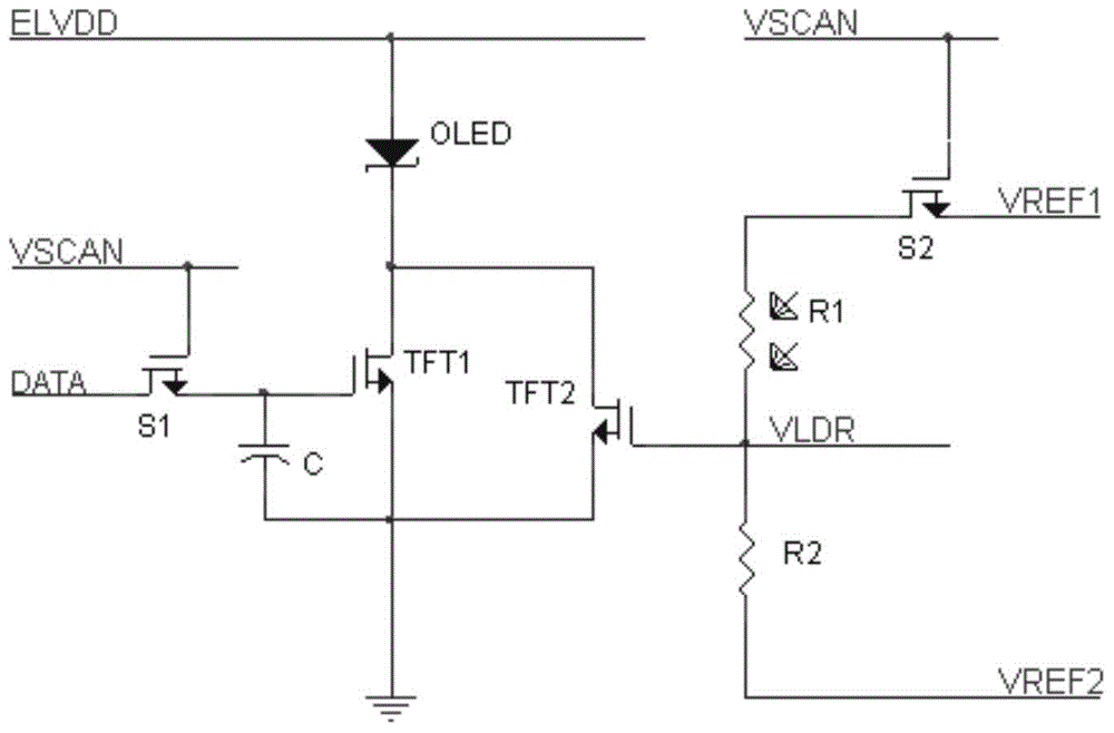
[0064] This embodiment provides an OLED pixel circuit, which uses a negative coefficient photoresistor to compensate the driving circuit of the N-type thin film transistor. The specific circuit structure is as follows: image 3 , 4 shown.

[0065] In the OLED pixel circuit, the synchronous transistor S2 and the compensating driving tube TFT2 are N-type thin film transistors, and the photosensitive resistor R1 is a negative coefficient photosensitive resistor whose resistance value decreases with the enhancement of the OLED brightness, and the free end of the series branch is the photosensitive resistor R1 One end of the voltage dividing resistor R2 is not connected. For negative coefficient photoresistors, the resistance value shows a large resistance value under the condition of no light; under the condition of light, the resistance value becomes smaller and the resistance value becomes smaller as the light increases.

[0066] image 3 Shown is a structure in which N-type ...

Embodiment 3

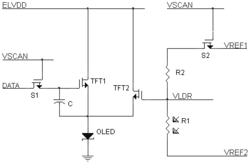
[0076] This embodiment provides an OLED pixel circuit, which uses a positive coefficient photoresistor to compensate the driving circuit of the P-type thin film transistor. The specific circuit structure is as follows: Figure 5 , 6 shown.

[0077] In the OLED pixel circuit, the synchronous transistor S2 and the compensating driving tube TFT2 are P-type thin film transistors, the photoresistor R1 is a positive-coefficient photoresistor whose resistance value increases with the brightness of the OLED, and the free end of the series branch is the photoresistor R1 One end of the voltage dividing resistor R2 is not connected.

[0078] Figure 5Shown is a structure in which a P-type thin film transistor is used in the OLED pixel circuit, and the compensation unit uses a positive coefficient photoresistor R1 to measure light on the OLED; in the drive unit, the first pole of the output transistor TFT1 is connected to the first input voltage terminal and the storage capacitor The s...


PUM


Abstract

The invention belongs to the technical field of display and specifically relates to an OLED pixel circuit and a display device thereof. The OLED pixel circuit comprises an OLED, a driving unit for driving the OLED to emit light, and a compensating unit. One electrode of the OLED is connected with the driving unit. The compensating unit comprises a sensing element capable of sensing light and converting an optical signal of the OLED into an electric signal, and reversely compensates the driving current applied by the driving unit to the OLED according to the light-emitting brightness of the OLED. The OLED pixel circuit, by means of the cooperation of a photosensitive resistor and a compensating driving transistor, compensates uneven light emitting of a display panel due to parameter drifting of the driving unit and OLED aging in the TFT-OLED pixel circuit. The display device using the OLED pixel circuit has a better display effect.

Description

technical field [0001] The invention belongs to the field of display technology, and in particular relates to an OLED pixel circuit and a display device thereof. Background technique [0002] In the existing TFT-OLED pixel circuit, there are changes in OLED current caused by uncontrollable factors such as process instability, parameter drift and device aging of TFT and OLED light-emitting devices, which in turn leads to uneven light emission of the display panel. [0003] In order to solve the problem of non-uniform luminescence, the existing electrical compensation methods usually use detection of voltage / current signals acting on the OLED to perform compensation. This compensation method can usually solve the problem of uneven luminescence caused by changes in the characteristics of the TFT drive tube, but it cannot solve the problem of inconsistent brightness caused by the aging of the OLED device itself or the difference in characteristics, even if the passing current of...

Claims


Application Information

Patent Timeline
IPC IPC(8): G09G3/32
CPCG09G3/3233G09G3/32G09G3/3208G09G2300/0842G09G2310/0251G09G2310/0262G09G2320/0233G09G2320/043G09G2320/045G09G2360/145
Inventor 宋琛
Owner BOE TECH GRP CO LTD
Why Eureka
Try Eureka