Wafer cleaning method

A wafer and megasonic technology, applied in cleaning methods and utensils, cleaning methods using liquids, chemical instruments and methods, etc., can solve problems such as scrapping, structural layer damage, long influence time, etc. Effect

Inactive Publication Date: 2015-09-09
ACM RES SHANGHAI
View PDF7 Cites 12 Cited by
  • Summary
  • Abstract
  • Description
  • Claims
  • Application Information

AI Technical Summary

Problems solved by technology

[0004] When the existing single-wafer cleaning device cleans the wafer, the ultrasonic or megasonic generator moves at a constant speed from the edge of the wafer to the center of the wafer and then stops. Therefore, during the entire cleaning process of the wafer, the center of the wafer The point is affected by the ultrasonic or megasonic energy for the longest time, which causes the structural layer at the center point of the wafer to be damaged, especially when the dielectric layer is cleaned, the dielectric layer at the center point of the wafer appears pits , resulting in reduced product yield or even scrapped

Method used


Image

  • Wafer cleaning method
  • Wafer cleaning method
  • Wafer cleaning method

Examples


Embodiment Construction

[0020] In order to describe the technical content, achieved goals and effects of the present invention in detail, the following will be described in detail in conjunction with the embodiments and accompanying drawings.

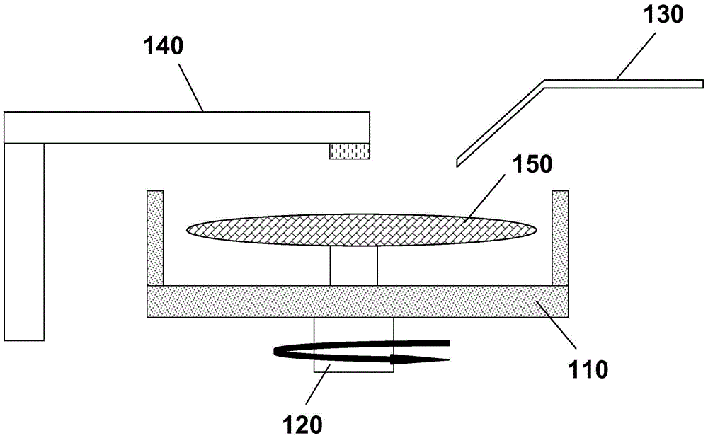
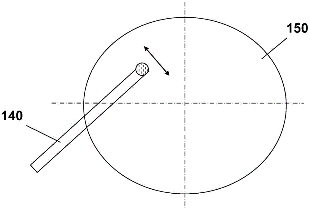
[0021] refer to figure 1 , figure 1 It is a structural schematic diagram of an exemplary embodiment of a wafer cleaning device. like figure 1 As shown, the wafer cleaning device includes a cleaning chamber 110 , a carrier 120 , a chemical solution supply pipeline 130 and a megasonic generator 140 . When using the wafer cleaning device to clean the wafer, the wafer 150 is placed on the carrier 120, the carrier 120 rotates, the wafer 150 rotates with the carrier 120, and the chemical solution supply pipeline 130 supplies chemicals to the surface of the wafer 150. liquid, the megasonic wave generator 140 is arranged above the surface of the wafer 150, and the megasonic wave generator 140 swings above the surface of the wafer 150, as figure 2 as shown, figu...


PUM


Abstract

The invention discloses a wafer cleaning method. A mega-sonic generator is utilized to clean the surface of a wafer. The method comprises the steps that the wafer is rotated and the mega-sonic generator is enabled to move between the edge of the wafer and the center of the wafer in a reciprocating way, and energy density distribution of the mega-sonic generator on the surface of the wafer is changed in the movement process of the mega-sonic generator. The energy density distribution of the mega-sonic generator on the surface of the wafer is changed so that mega-sonic energy affected by the center point of the wafer is enabled to be consistent with mega-sonic energy affected by other positions of the wafer, and thus damage to the structural layer of the center point of the wafer in the cleaning process or generation of pits at the center of the wafer can be avoided.

Description

technical field [0001] The invention relates to the field of integrated circuit manufacturing, in particular to a wafer cleaning method. Background technique [0002] Cleaning is the process of using physical, chemical or mechanical methods to desorb the pollutants adsorbed on the wafer surface and leave the wafer surface. With the rapid development of integrated circuit technology and the continuous reduction of critical dimensions of graphics, as well as the introduction of new materials, in the process of integrated circuit manufacturing, the quality of cleaning has seriously affected the performance, reliability and stability of advanced electronic devices. At present, wafer cleaning is still dominated by wet cleaning, and the traditional batch cleaning technology in wet cleaning is difficult to adapt to wet cleaning driven by many process factors. Therefore, it is necessary to introduce new Cleaning process to meet process requirements. [0003] Single-wafer cleaning ...

Claims


Application Information

Patent Timeline
Patent Type & Authority Applications(China)
IPC IPC(8): H01L21/02B08B3/12
CPCH01L21/02057B08B3/12
Inventor 杨贵璞王坚王晖
Owner ACM RES SHANGHAI
Why Eureka
Try Eureka