Check patentability & draft patents in minutes with Patsnap Eureka AI!

An electrostatic discharge protection circuit

An electrostatic discharge protection and circuit technology, applied in circuits, electrical components, electric solid devices, etc., can solve problems such as diode damage, internal component collapse, and increased difficulty, and achieve the effect of solving ESD, low parasitic and stray capacitance

Active Publication Date: 2018-02-09
MICROCHIP TECH INC
View PDF5 Cites 0 Cited by
  • Summary
  • Abstract
  • Description
  • Claims
  • Application Information

AI Technical Summary

Problems solved by technology

However, using a diode as an ESD protection circuit can only provide forward ESD current protection, so it is very easy to cause internal components to collapse due to excessive cross-voltage, and then damage the diode; and with the miniaturization of the manufacturing process, the breakdown voltage of the components themselves It also decreases, which increases the difficulty of design
[0008] In addition, because the receiving terminal pin (RX pin) will have a signal like a swing (Swing), so the trigger voltage cannot be too low, and a situation similar to clipping will occur.

Method used


Image

  • An electrostatic discharge protection circuit
  • An electrostatic discharge protection circuit
  • An electrostatic discharge protection circuit

Examples


Embodiment Construction

[0035] Although the present invention can be embodied in different forms, those shown in the drawings and described below are preferred embodiments of the present invention, and please understand that what is disclosed herein is considered an example of the present invention, and It is not intended to limit the invention to the particular embodiments shown and / or described.

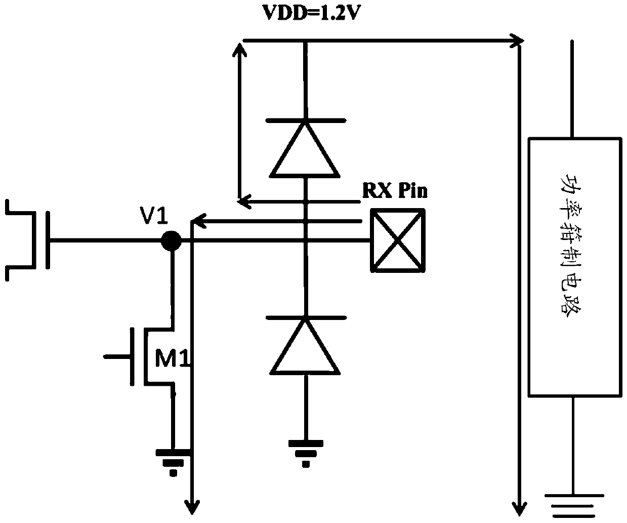
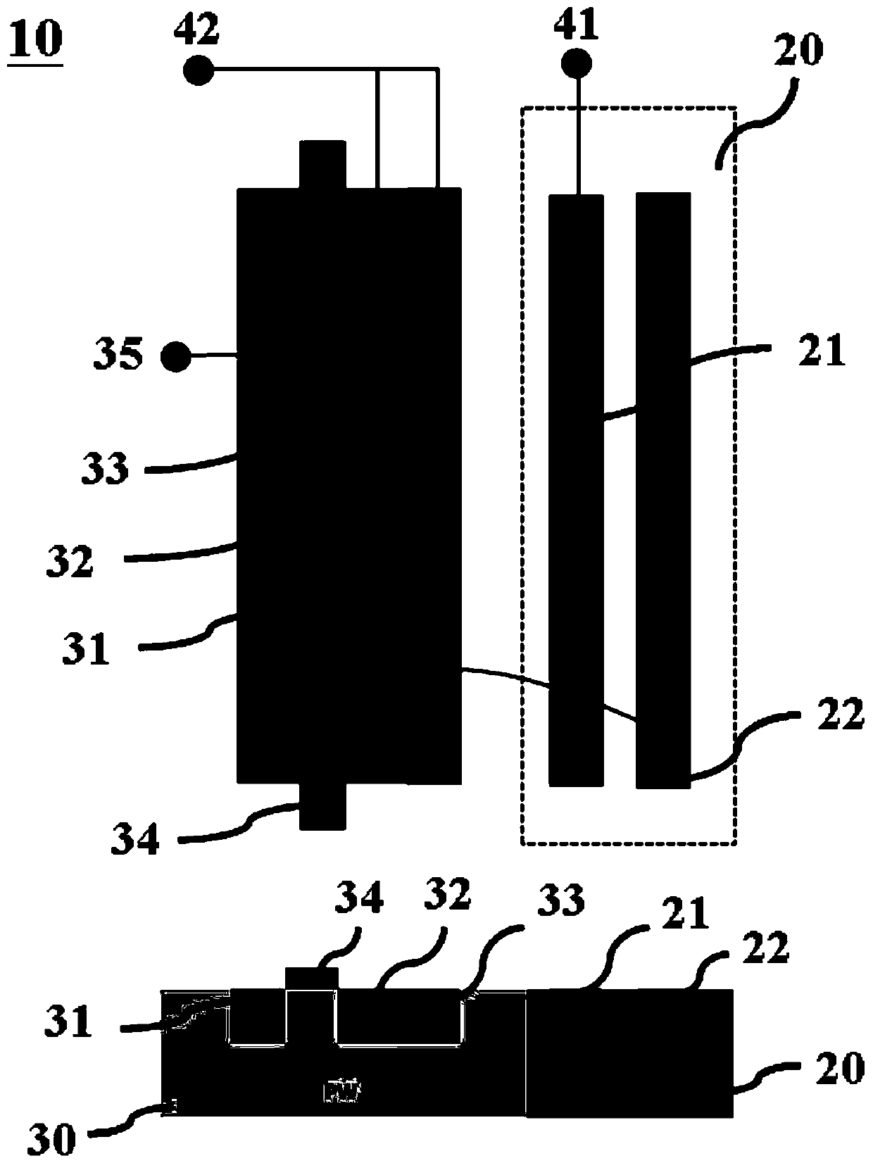
[0036] Please refer now image 3 , is the first embodiment of the layout of the ESD protection circuit of the present invention. An electrostatic discharge protection circuit 10 is composed of a diode and a metal oxide semiconductor device disposed on a semiconductive substrate. An electrostatic discharge protection circuit 10 includes: a first well region 20 having a first conductive form; a second well region 30 adjacent to the first well region and having a second conductive form; a first high-concentration doped region 21 , located in the first well region 20 and having a second conductive form, the...


PUM


Abstract

The present invention discloses an electrostatic discharge protection circuit, comprising a diode and a N-type metal-oxide-semiconductor (NMOS) transistor. The diode locating on a N-well comprises an high P-doping concentration region and an nonadjacent high N-doping concentration region. The NMOS transistor, locating on a P-well, comprises a drain, a source and a gate, and the drain and the source are formed by the high N-doping concentration region. Wherein the P-well further comprises a high P-doping concentration region near the source, the drain of the NMOS is electrically connected to the high N-doping concentration region of the diode, the source of the NMOS and the adjacent high P-doping concentration region are electrically connected to a ground, the gate of the NMOS transistor electrically connected to a trigger point. Accordingly, the electrostatic discharge protection circuit has a low parasitic capacitance, wide operating voltage range and high electrostatic discharge (ESD) capability for resolving the problems about the ESD of the RX pins.

Description

technical field [0001] The invention relates to an electrostatic discharge protection circuit, in particular to an electrostatic discharge protection circuit using a silicon controlled rectifier, which has low stray capacitance, low trigger voltage, high tolerance voltage operating range and high ESD capability. Background technique [0002] In order to prevent integrated circuit (Integrated circuit, IC) from being damaged by Electrostatic discharge (ESD) bombardment in the process of manufacturing, production and use, it is necessary to add ESD protection on any path connected to the bonding wire circuit, in order to conduct the ESD current to avoid damage to the internal circuit. [0003] Generally speaking, protection circuits can be classified into diodes, metal oxide semiconductor (MOS) transistors, silicon controlled rectifiers (Silicon Controlled Rectifier, SCR), etc. Among them, the silicon controlled rectifier has the highest ESD current conduction capability under...

Claims


Application Information

Patent Timeline
Patent Type & Authority Patents(China)
IPC IPC(8): H01L27/02
CPCH01L27/0255H01L27/0266
Inventor 陈哲宏
Owner MICROCHIP TECH INC
Features
  • R&D
  • Intellectual Property
  • Life Sciences
  • Materials
  • Tech Scout
  • Unparalleled Data Quality
  • Higher Quality Content
  • 60% Fewer Hallucinations
Learn More