
A Voltage Stabilizer Circuit Based on Slew Rate Enhancement
A voltage-stabilizing circuit and slew rate-enhancing technology, applied in the direction of regulating electrical variables, control/regulating systems, instruments, etc., can solve the problems of unsuitable linear voltage regulators with high power supply voltage and cannot respond immediately, and achieve optimal output transient Features, simplified circuit, area saving effect
- Summary
- Abstract
- Description
- Claims
- Application Information
AI Technical Summary
Problems solved by technology
Method used
Image

Examples
Embodiment Construction
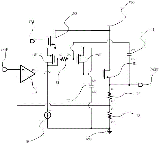
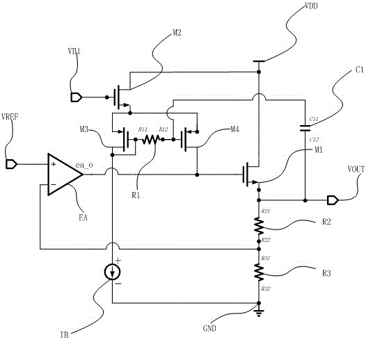
[0016] The solution of the present invention will be described in detail below in combination with the preferred embodiments thereof. The invention directly connects the output voltage VOUT to the grid stage of the M4 tube by using the capacitor device, so as to realize the zero-delay loop response. At the same time, M3, R1, and IB are used to provide static voltage bias for the gate of M4, and Native NMOS transistors M2 and C2 are used to provide static voltage bias for the source of M4 to ensure that the circuit achieves zero-delay loop response and has high performance. Power supply voltage rejection ratio, suitable for low input voltage application environment and other advantages. The output stage uses Native NMOS as the output power MOS tube, which has the advantage of obtaining a higher power supply voltage rejection ratio than the PMOS tube commonly used in existing solutions.
[0017] figure 2 A structural schematic diagram of a voltage regulator based on a slew ra...
PUM
 Abstract
Description
Claims
Application Information