Gaas-based phemt device and preparation method thereof
A technology of devices and barrier layers, applied in semiconductor/solid-state device manufacturing, semiconductor devices, electrical components, etc., to achieve the effect of improving gate-drain breakdown voltage and low process difficulty
- Summary
- Abstract
- Description
- Claims
- Application Information
AI Technical Summary
Problems solved by technology
Method used
Image
Examples
Embodiment Construction
[0020] The following will clearly and completely describe the technical solutions in the embodiments of the present invention with reference to the accompanying drawings in the embodiments of the present invention. Obviously, the described embodiments are only some, not all, embodiments of the present invention. Based on the embodiments of the present invention, all other embodiments obtained by persons of ordinary skill in the art without making creative efforts belong to the protection scope of the present invention.
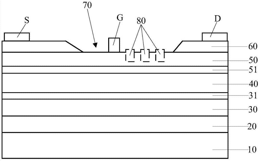
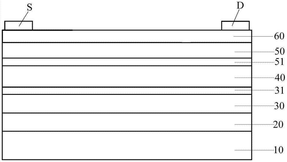
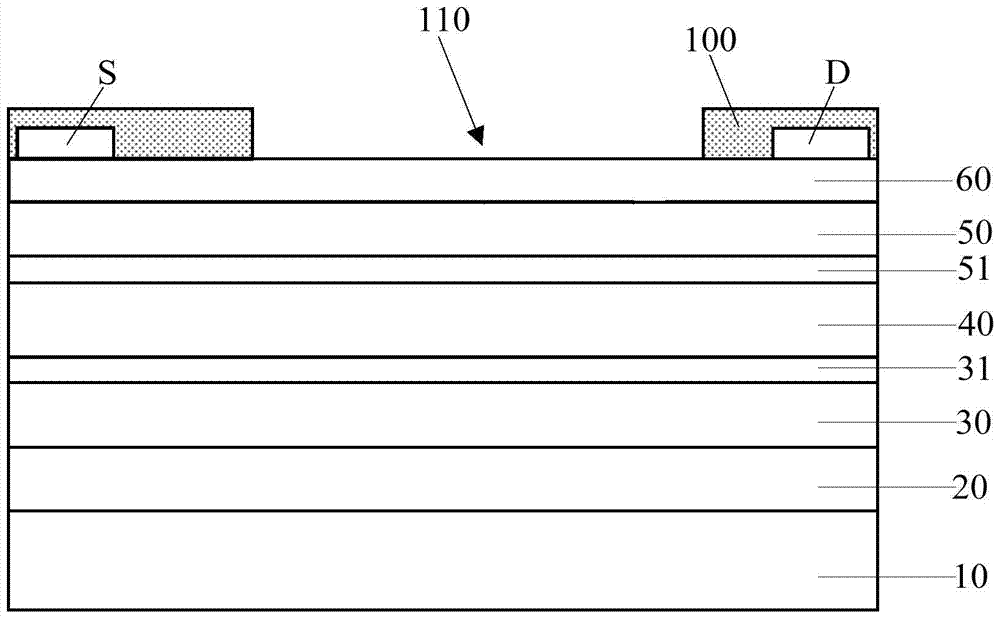
[0021] see figure 1 , is a schematic cross-sectional view of a GaAs-based pHEMT device according to an embodiment of the present invention. The GaAs-based pHEMT device of this embodiment includes a GaAs substrate 10, a buffer layer 20, a first AlGaAs barrier layer 30, an InGaAs channel layer 40, a second AlGaAs barrier layer 50, and N + - GaAs layer 60 . The first AlGaAs barrier layer 30 and the InGaAs channel layer 40 form a two-dimensional electron gas 31 ...
PUM
 Abstract
Description
Claims
Application Information


