Dual-band band-rejection filter based on defected microstrip structure and defected ground structure
A technology of defective ground structure and band-rejection filter, which is applied in waveguide devices, electrical components, circuits, etc., can solve the problems that the selection characteristics need to be improved, the volume is large, and the independent adjustment cannot be realized, and the structure is compact and the selection characteristics are improved. , to meet the effect of miniaturization
- Summary
- Abstract
- Description
- Claims
- Application Information
AI Technical Summary
Problems solved by technology
Method used
Image
Examples
Embodiment 1
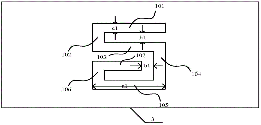
[0039] Embodiment 1 of the present invention: a dual-band band-stop filter based on a defective microstrip structure and a defective ground structure, such as figure 1 , figure 2 , Figure 5 , Figure 6 , Figure 12 As shown, it includes: a dielectric substrate 1, a metal plated ground plate 2 disposed on the bottom surface of the dielectric substrate 1, and a metal microstrip line 3 disposed on the dielectric substrate 1, and the ground plate 2 and the microstrip line 3 are engraved with The corrosion has a δ-shaped defect structure. Both the ground plate 2 and the microstrip line 3 are etched with two δ-shaped defect structures, the two δ-shaped defect structures on the ground plate 2 are cascaded, and the two δ-shaped defect structures on the microstrip line 3 couplet. The δ-shaped defect structure is a δ-shaped groove, including A groove line 101, B groove line 102, C groove line 103, D groove line 104, E groove line 105, F groove line 106 and G groove line 107. The...
Embodiment 2
[0040] Embodiment 2: A dual-band band-rejection filter based on a defective microstrip structure and a defective ground structure, including: a dielectric substrate 1, a metal-plated ground plate 2 disposed on the bottom surface of the dielectric substrate 1, and a metal microstructure disposed on the dielectric substrate 1. The stripline 3, the ground plate 2 and the microstrip line 3 are all etched with δ-shaped defect structures. Both the ground plate 2 and the microstrip line 3 are etched with two δ-shaped defect structures, the two δ-shaped defect structures on the ground plate 2 are cascaded, and the two δ-shaped defect structures on the microstrip line 3 couplet. The δ-shaped defect structure is a δ-shaped groove, including A groove line 101, B groove line 102, C groove line 103, D groove line 104, E groove line 105, F groove line 106 and G groove line 107. The two ends of the B slot line 102 are respectively connected with one end of the A slot line 101 and the C slot...
Embodiment 3
[0041]Embodiment 3: A dual-band band-rejection filter based on a defective microstrip structure and a defective ground structure, including: a dielectric substrate 1, a metal-plated ground plate 2 disposed on the bottom surface of the dielectric substrate 1, and a metal microstrip disposed on the dielectric substrate 1. The stripline 3, the ground plate 2 and the microstrip line 3 are all etched with δ-shaped defect structures. The δ-shaped defect structure is a δ-shaped groove, including A groove line 101, B groove line 102, C groove line 103, D groove line 104, E groove line 105, F groove line 106 and G groove line 107. The two ends of the B slot line 102 are respectively connected with one end of the A slot line 101 and the C slot line 103, the two ends of the D slot line 104 are respectively connected with one end of the E slot line 105 and the other end of the C slot line 103, and the F slot line The two ends of line 106 are connected with one end of G groove line 107 and...
PUM
| Property | Measurement | Unit |
|---|---|---|
| Thickness | aaaaa | aaaaa |
Abstract
Description
Claims
Application Information


