Display substrate and manufacturing method therefor and display device

A display substrate and manufacturing method technology, applied in semiconductor/solid-state device manufacturing, electrical components, electrical solid-state devices, etc., can solve the problems of light leakage, light color, light output rate and color purity of OLED display devices, and optoelectronic properties of components.

Inactive Publication Date: 2015-10-14
BOE TECH GRP CO LTD
View PDF4 Cites 44 Cited by
  • Summary
  • Abstract
  • Description
  • Claims
  • Application Information

AI Technical Summary

Problems solved by technology

However, the pixel defining layer 40 is generally formed of a light-transmitting material, and the side light emitted by the light-emitting layer will enter into adjacent sub-pixels, for example figure 1 The side light 21 emitted by the light-emitting layer of the red sub-pixel R shown will be incident on the adjacent green sub-pixel G, which will cause light leakage and light color interference, resulting in a decrease in the light extraction rate and color purity of the OLED display device.
[

Method used


Image

  • Display substrate and manufacturing method therefor and display device
  • Display substrate and manufacturing method therefor and display device
  • Display substrate and manufacturing method therefor and display device

Examples


Embodiment 1

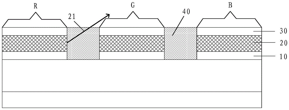
[0023] An embodiment of the present invention provides a display substrate, referring to Figure 2-3 As shown, the display substrate includes: a transparent substrate 50, a pixel defining layer 40 formed on the transparent substrate 50, and a light emitting layer 20 located in the sub-pixel region defined by the pixel defining layer 40; the pixel defining layer 40 includes: a reflective Layer 41, the reflective layer 41 is convex toward the light-emitting side of the display substrate, and is used to reflect the light emitted from the light-emitting layer to the reflective layer to the light-emitting side of the display substrate; in the area where the pixel defining layer is located, from the reflective layer to the display substrate The light-emitting side part is transparent.

[0024] In the above display substrate, the embodiment of the present invention does not limit the material of the light-emitting layer, for example, the material of the light-emitting layer may be an...

Embodiment 2

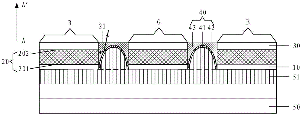
[0033] An embodiment of the present invention provides a display substrate, referring to figure 2 As shown, the display substrate includes: a transparent substrate 50, a pixel defining layer 40 formed on the transparent substrate 50, and a light emitting layer 20 located in the sub-pixel region defined by the pixel defining layer 40; the pixel defining layer 40 includes: a reflective Layer 41, the reflective layer 41 is convex toward the light-emitting side of the display substrate, and is used to reflect the light emitted from the light-emitting layer to the reflective layer to the light-emitting side of the display substrate; the pixel defining layer 40 also includes: The projection 42, the reflective layer 41 covers all or part of the projection 42, and the first transparent portion 43 located on the reflective layer 41; the light-emitting side of the display substrate is the surface of the display substrate away from the transparent substrate.

[0034] In the above displa...

Embodiment 3

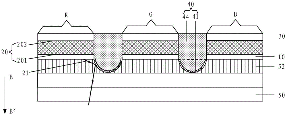
[0043] An embodiment of the present invention provides a display substrate, referring to image 3 As shown, the display substrate includes: a transparent substrate 50, a pixel defining layer 40 formed on the transparent substrate 50, and a light emitting layer 20 located in the sub-pixel region defined by the pixel defining layer 40; the pixel defining layer 40 includes: a reflective Layer 41, the reflective layer 41 is convex toward the light-emitting side of the display substrate, and is used to reflect the light emitted from the light-emitting layer to the reflective layer to the light-emitting side of the display substrate; the display substrate also includes a second transparent layer on the transparent substrate 50 layer 52, the second transparent layer 52 is formed with a groove in the area where the pixel defining layer 40 is located, and the reflective layer 41 covers all or part of the groove; the pixel defining layer 40 also includes: a second transparent portion 44 ...


PUM


Abstract

The invention provides a display substrate and a manufacturing method therefor and a display device and relates to the technical field of display. The display device comprising the display substrate can be used for effectively improving the problem of light leakage and photochromic interference. The light out-coupling efficiency and the color purity of the display device are effectively improved. The display substrate comprises a transparent substrate, a pixel defining layer formed on the transparent substrate and a light emitting layer located in a subpixel region defined by the pixel defining layer, wherein the pixel defining layer comprises a reflective layer which is protruding toward the light out side of the display substrate for reflecting the light emitted from the light emitting layer to the reflective layer to the light out side of the display substrate; in a region of the pixel defining layer, part of the light out side of the display substrate from the reflective layer is transparent. The invention further provides manufacturing methods of the display substrate as well as the display device comprising the display substrate.

Description

technical field [0001] The invention relates to the field of display technology, in particular to a display substrate, a manufacturing method thereof, and a display device. Background technique [0002] OLED (Organic Light Emitting Diode, Organic Light Emitting Diode) display has the characteristics of fast response speed, high contrast ratio, wide viewing angle, etc., and is considered to be the next generation display technology. [0003] The OLED display includes a packaging substrate and a substrate substrate, and the substrate substrate includes pixel units arranged in an array, such as figure 1 As shown, each pixel unit includes a red sub-pixel R, a green sub-pixel G, and a blue sub-pixel B, and each sub-pixel includes an anode 10, a light-emitting layer 20, and a cathode 30. Usually, pixels are formed between adjacent sub-pixels. The boundary layer 40 is used to prevent the light emitted from the light-emitting layers of adjacent sub-pixels from influencing each othe...

Claims


Application Information

Patent Timeline
IPC IPC(8): H01L27/32H01L51/52H01L51/56
CPCH10K59/173H10K59/122H10K50/856H10K71/00H10K59/1201
Inventor 崔颖胡春静
Owner BOE TECH GRP CO LTD
Why Eureka
Try Eureka