Chip scale package LED packaging method
A technology of chip-level packaging and packaging methods, applied in the direction of electrical components, circuits, semiconductor devices, etc., can solve problems such as unsuitable for large-scale production, complicated packaging process, and huge manpower and material resources
- Summary
- Abstract
- Description
- Claims
- Application Information
AI Technical Summary
Problems solved by technology
Method used
Image

Examples
Embodiment 1
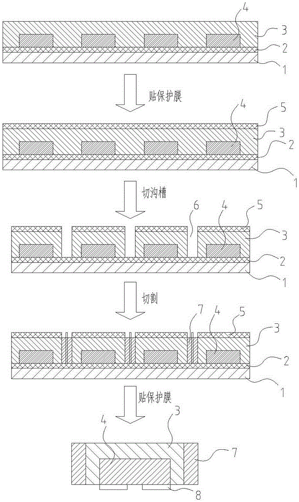
[0026] like figure 1 Shown, a kind of package method of chip-scale package LED comprises the following steps:
[0027] (1) A layer of fixed film 2 for fixing the position of the LED chip 4 is arranged on the carrier plate 1; the fixed film 2 of this embodiment is a UV double-sided tape film, and the carrier plate 1 is a glass plate; the UV double-sided tape film can be It is directly fixed on one side of the glass plate by pasting, and then the UV double-sided tape film can be separated from the glass plate by irradiating the other side of the glass plate;
[0028] (2) A number of LED chips 4 are distributed on the surface of the fixed film 2. The number of LED chips 4 can be set according to the size of the glass plate, or according to production requirements. The LED chips 4 are distributed in an array, and the adjacent LED chips There are gaps for cutting between 4, and the width of each gap is consistent to ensure the consistency of each LED after cutting; the LED chip 4 ...
Embodiment 2
[0036] like figure 1 Shown, a kind of package method of chip-scale package LED comprises the following steps:
[0037] (1) A layer of fixing film 2 for fixing the position of the LED chip 4 is arranged on the carrier plate 1; the fixing film 2 of this embodiment is a heat-separation tape film, and the carrier plate 1 is a glass plate; the heat-separation tape film can be directly passed through The pasting method is fixed on one side of the glass plate, and then the carrier plate 1 can be heated to separate the thermal separation tape film from the carrier plate 1;
[0038] (2) A number of LED chips 4 are distributed on the surface of the fixed film 2. The number of LED chips 4 can be set according to the size of the glass plate, or according to production requirements. The LED chips 4 are distributed in an array, and the adjacent LED chips There are gaps for cutting between 4, and the width of each gap is consistent to ensure the consistency of each LED after cutting; the LE...
PUM
| Property | Measurement | Unit |
|---|---|---|
| Width | aaaaa | aaaaa |
Abstract
Description
Claims
Application Information
 - Generate Ideas
- Intellectual Property
- Life Sciences
- Materials
- Tech Scout
- Unparalleled Data Quality
- Higher Quality Content
- 60% Fewer Hallucinations
Browse by: Latest US Patents, China's latest patents, Technical Efficacy Thesaurus, Application Domain, Technology Topic, Popular Technical Reports.
© 2025 PatSnap. All rights reserved.Legal|Privacy policy|Modern Slavery Act Transparency Statement|Sitemap|About US| Contact US: help@patsnap.com